Label-Free Chemical Detection in Micro-Fabricated Devices Using FT-IR Spectroscopic Imaging
Spectroscopy
Fourier transform infrared (FT-IR) spectroscopic imaging is a highly versatile technique that can be applied to a wide range of systems. This article summarizes some of the recent efforts developing applications of FT-IR imaging for microfluidics. The main advantage of FT-IR imaging compared to traditional imaging methods is that it is a label-free imaging technique.
Fourier transform infrared (FT-IR) spectroscopic imaging is a highly versatile technique that can be applied to a wide range of systems. This article summarizes some of the recent efforts developing applications of FT-IR imaging for microfluidics. The main advantage of FT-IR imaging compared to traditional imaging methods is that it is a label-free imaging technique. There is no need to develop tags or labels, multiple components are simultaneously traced, and images can be taken without disturbing the sample. All of these advantages are accompanied with a near-video frame rate acquisition speed. Different approaches to obtain FT-IR images (transmission and attenuated total reflection mode) of microfluidic devices are discussed including novel ways to create microfluidic devices.
Microfluidic technology is a powerful tool that has a wide range of applications in chemical and biological analysis (1). The improved heat and mass transfer in microfabricated systems in comparison to traditional processes provides the opportunity to increase control over the yield, the speed of the turnover of experiments for high-throughput studies, and reduce the amount of precious reagents used (2). Knowing the chemical composition at a specific point in the microfabricated device can aid in the design and optimization of these devices (3,4).
Detection in microfabricated devices often relies on additional tracers or tags to visualize the existence and the distribution of particular components. One of the most widely used methods is confocal fluorescence microscopy. The advantage of fluorescence is that it is highly sensitive (5) and can often achieve sufficient spatial resolution. However, finding a suitable fluorescence agent and photobleaching are some of the remaining challenges to overcome. The tracer also has to be inert enough that it will not decompose or interfere with the process of interest (for example, chemical reactions and diffusion). Raman, surface-enhanced Raman spectroscopy (SERS), and coherent anti-Stokes Raman scattering (CARS) have been shown as promising label-free detection methods in microfluidic systems (6–10). In this article, we discuss some recent studies that have demonstrated that Fourier transform infrared (FT-IR) spectroscopic imaging can be a powerful detection tool, as was proposed earlier (11), to extract spatially resolved rich chemical information from microfluidic devices in a label-free manner.
FT-IR Spectroscopic Imaging
FT-IR imaging has been used as a highly versatile analytical method, providing spatially resolved, chemically specific information for studying multicomponent systems (12). Recently, conventional FT-IR microscopy using a single-element detector was applied to analyze fast reactions in microfluidic flows where spectral information from a specific location in a channel was obtained (13). FT-IR spectroscopic imaging combines the benefits of imaging and spectroscopy providing chemical maps of studied samples. The chemical specificity comes from the intrinsic molecular vibrations, revealed by spectral bands, while spatial information is collected from the focal plane array (FPA) detectors. An FPA detector comprises thousands of detector pixels, each collecting an infrared spectrum so that thousands of infrared spectra are collected simultaneously in a single imaging measurement. This approach reduces the time required to collect all the spectral data when compared to point-to-point mapping using a single element detector with apertures (14).
Characteristic spectral bands can then be used as markers for specific components, which allows their distribution within the imaged area to be revealed. Multivariate methods are also available to separate components with similar spectral features to generate representative maps for each component. A full mid-IR spectrum (4000–900 cm-1) is collected from each detector pixel, and multiple components can be simultaneously tracked in one single imaging measurement either using univariate or multivariate approaches. This multicomponent imaging feature is a significant advantage compared to ordinary fluorescence measurements in which only one component is traced at a time. The absorbance of a spectral band is directly correlated to the concentration of the component so that results obtained can be quantified.
Because all spectra are collected simultaneously, FT-IR imaging using FPA detectors is suitable for studying dynamic systems such as diffusion and dissolution (15–20) and has great potential for high-throughput applications, especially when combined with the attenuated total reflection (ATR) sampling method (11,21).
ATR Imaging
In the ATR approach, the infrared light is totally internally reflected at the interface between the high refractive index infrared-transparent element and the lower refractive index medium (the sample). Common elements used for ATR measurement are diamond (n ≈ 2.4), ZnSe (n ≈ 2.4), Si (n ≈ 3.4), or Ge (n ≈ 4). In this measurement mode, the infrared light probes into the sample as an evanescence wave, the field strength of which decays exponentially into the sample. The depth of penetration is on the order of a few micrometers and the resultant pathlength (the equivalent pathlength) is also in the order of several micrometers depending on the refractive indices of the sample, the ATR element, and the incident angle. The ATR element is selected such that it will provide a relatively small, but known, pathlength that will produce an appropriate on-scale absorbance. Other considerations include the physical and chemical properties of the ATR element for specific applications. The generally small pathlength from ATR mode measurement offers the opportunity to measure materials that have strong mid-IR bands such as water and reduces sample preparation because no microtoming or polishing of the sample is required. The possibility of acquiring spectra using ATR mode increases the applicability to study samples in situ and to monitor processes on line. The simplicity of measurement allows rapid analysis of an array of deposited samples in the imaging area (11,21–23).
Combined FT-IR Imaging and Microfluidics
ATR Mode
Because the evanescent wave probes a relatively shallow layer, the sample must be in close contact with the ATR element to be exposed to and interact with this evanescent wave. This sampling requirement for ATR measurement is automatically satisfied when the sample being measured is a fluid. FT-IR imaging in ATR mode is therefore suitable to study microfluidic systems. Microfluidic devices are often made of polydimethylsiloxane (PDMS) using templates in which channels are created when the PDMS stamp is bonded to a flat surface such as glass. With ATR FT-IR imaging, instead of bonding the PDMS device to glass, the PDMS device is bonded to the imaging surface of the ATR element so that the measuring surface forms one of the walls of the microfluidic channel. The fluid flowing inside the channel that comes to close proximity with the surface of the ATR element is measured.
Figure 1: Top left: The "Y-junction" PDMS microfluidic device. Middle: The PDMS microfluidic device on the ATR imaging surface. Imaging area is indicated by the red rectangle. Bottom right: RGB imaging of a Y-junction microfluidic device with water entering from the right and PEG 200 entering from the left measured with macro ATR FT-IR imaging. Red, blue, and green represent the presence of PDMS, water, and PEG 200, respectively. The imaging area is 2.56 mm × 3.58 mm.
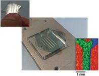
ATR elements are often expensive and cannot be used as disposable units; therefore, the bonding of PDMS onto the ATR surface must be reversible. PDMS will bond weakly with a clean, oil-free surface. However, most microfluidic experiments cannot rely on this weak bonding as the seal for the channels because pressure from the fluid will cause liquid to escape by overcoming this weak adhesion force. Fortunately, this issue can be easily rectified. A rigid poly(methyl methacrylate) (PMMA) sheet (or any rigid, ideally transparent material for visible inspection) can be used as a press to provide a stronger bonding between the PDMS and the ATR element. One of the inherent advantages of ATR imaging measurements is that the presence of foreign particles (dust) that may affect contact quality between the PDMS chip and the ATR surface can be easily detected (24). Leakage of fluids through the gap between the ATR surface and the PDMS chip can also be detected from the image as the escaped fluid will be in contact with the ATR element. Figure 1 shows the typical "Y-junction" PDMS microfluidic device that we have used as the first test of the principle (25). An image of the device can be generated based on the band specific to PDMS. When two different fluids are injected from the two entrances of the microfluidic device, the mixing between the two fluids can be studied. As an illustration, we injected water (75 μL/h) through the right entrance and PEG 200 (25 μL/h) through the left channel. Because both fluids are transparent in visible range, it was not possible to visualize the flow pattern using visible light without adding dye to the solution. Using ATR FT-IR imaging, the two fluids are easily distinguished. Water can be traced using the ν(O-H) band at 3700–3100 cm-1, and PEG 200 can be traced using the characteristic ν(C-H) bands at 3000–2800 cm-1. A red-green-blue (RGB) figure (Figure 1) has been created to show the distribution of PDMS (red), water (blue), and PEG (green). The image allows us to immediately identify the effect of viscosity to the flow pattern. The water stream, despite having a higher flow rate, was constrained to the right while most of the channel was occupied by the PEG 200 because of the difference between their viscosities.
Transmission Mode
There are both advantages and disadvantages to working in transmission mode. One of the main advantages is that the whole volume of the fluid is analyzed as compared to the first few micrometers from the surface in ATR mode. However, for the same reason, one of the main disadvantages is that the fluid thickness is often limited to ~10 μm to ensure that most of the spectral bands are within the linear detection limit (around 0.8 absorbance units). For the stronger spectral bands such as the band from water ν(O-H) mode, the thickness may need to be further reduced to 2–3 μm. In general, therefore, certain parts of the spectral region will not be accessible in transmission with a workable pathlength when the fluid studied has strong spectral bands.
To study in transmission mode, the top and bottom layer of the microfluidic device has to be transparent in the infrared region. Common infrared-transparent materials used for making spectroscopic windows include BaF2, CaF2, and ZnSe. Hygroscopic materials such as NaCl and KBr are not suitable for this purpose because water will dissolve the window. Silicon is also transparent in the mid-IR region and has great potential for use as a material to construct microfluidic devices for FT-IR imaging because etching techniques for silicon wafers are well established and its surface properties can be tuned with self-assembled monolayers. Other infrared transparent windows are often not malleable and specific etching techniques may first need to be developed (26). Furthermore, these crystals are often too expensive to be used as a one-off device (a pair of large windows would cost as much as $320). The ability to create reusable microfluidic devices on these windows would be an important step forward for the wider application of this approach.
Wax-Printed Microfluidic Devices
One of the possibilities for producing microfludic devices is direct wax printing. Machines that can print molten wax droplets at precise locations are commercially available. Previous studies used wax printers in one of two ways, either to create the master, which was then used to cast PDMS devices to obtain the negative design of the printed features (27,28), or printing the device on paper to create paper microfluidics (29,30). Our wax printing approach manufactures microfluidic devices with free-flowing channels directly without the need for casting PDMS over the print. We have applied this method to create various microfluidic devices on a CaF2 substrate. The procedure is relatively straightforward. Microfluidic devices are first designed and programmed into the computer that operates the microdrop machine. Molten wax droplets, each of which has a controllable diameter of 30–70 μm, are printed directly onto the CaF2 window. The CaF2 window can be precoated with a thin layer of polymer to create a hydrophobic surface when necessary. The adjacent molten wax droplets join together and solidify to form a wax wall. Figure 2 shows a photograph of a T-junction microfluidic device created by the wax printing method.
Figure 2: A picture of the wax-printed microfluidic device before being sandwiched between the two CaF2 windows for imaging in transmission.
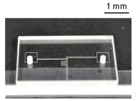
A spacer is added that determines the depth of the channel, which is also the pathlength of the measurement. The microfludic channel is created when another CaF2 window is pressed on top and held together by screws, for example. Experiments can be conducted immediately after the printing process, and the infrared-transparent windows can be reused because the wax channels can be removed easily. Depending on the complexity of the design, the printing time is typically less than 10 min. New microfluidic devices can be modified and created in a matter of minutes. The size of the wax droplet is on the order of 50 μm and the machine has an accuracy of 40 μm, which defines the resolution of the microfluidic device. So far, we have only experimented using wax that is vulnerable to many organic solvents and oil. However, waxes that are highly chemically resistant are also available; we plan to test these and present the results in the future.
Transflection mode
In transflection mode, the sample is placed on an infrared-reflective substrate surface where the IR radiation passes through the sample, is reflected off the surface of the substrate, and passes through the sample again before being collected with the sample objective. For microfluidic applications, the advantage of this approach is that only the top surface needs to be infrared transparent. When an open channel is used (that is, when the top surface is not covered and is open to air), there is no need to construct the microfluidic device in an infrared-transparent material. The main requirement is that the bottom of the channel is infrared reflective, which can be easily achieved. However, the thickness constraint that applies in transmission mode measurement is more severe because the pathlength is twice the thickness of the fluid. Nevertheless, such an approach was used in the study of biofilms and live cells in an open channel setting (31).
Two-Phase Segmented Flow
In comparison to laminar flow, segmented flow and droplet flow offer the possibility to perform high-throughput studies without increasing the size or complexity of the microfluidic device (32). Although each droplet or segment is compartmentalized by the immiscible inert phase, each segment can be considered as individual experiments.
Figure 3: Top figure: ATR FT-IR image of oil with water droplets flowing inside microfluidic channels taken with a snapshot at less than 50 ms scanning time with a frame rate of approximately 18 Hz. Imaging area to right of the FT-IR image: schematic diagram showing the side view of the moving water droplet in oil in the microfluidic device on the ATR element. Bottom figure: The blue line represents the extracted averaged ATR spectrum from the moving water droplet region and the red line represents the extracted averaged ATR spectrum from the oil region.
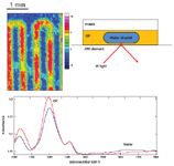
FT-IR imaging of droplets or segments can be captured easily when they are stationary. The applications of segmented flows include protein crystallization, live cells in droplets, and other slow processes. Many of these research ideas are yet to be realized in combination with FT-IR imaging. One of the main challenges in imaging segmented flows is when one wants to capture the droplet or segments while they are moving. The acquisition time for a typical FT-IR imaging measurement is on the order of seconds. Although this imaging speed is already a great improvement from the early FT-IR imaging systems; it is often not fast enough to capture the moving droplets. Fortunately, through optimization of the data acquisition process, FT-IR imaging of moving segments or droplets in microfluidic channels has been demonstrated (33). Traditionally, the acquired data in an FT-IR imaging measurement are the average of several scans to improve on the signal-to-noise ratio. (In theory, the signal-to-noise ratio is improved by the square root of the number of scans taken.) However, to capture droplet flow, only one scan can be collected. The time taken for one scan is governed by the spectral range and spectral resolution set in the experiment as well as the number of detector pixels used. For an imaging experiment with a 64 × 64 pixel array, 8 cm-1 spectral resolution, and 4000–900 cm-1 spectral range, the scanning time is approximately 600–700 ms. With current technology, one needs to reduce the amount of data collected to improve this speed. For example, most of the spectral information is contained in the so-called fingerprint region of the infrared spectrum (between 1800 and 500 cm-1). Because the detection limit for the FPA detector is around 900 cm-1 or ~1000 cm-1 when CaF2 is used as the substrate material, there is an opportunity to reduce the amount of data collected without losing significant chemical information by reducing the spectral range to 1800–1000 cm-1. This can increase the speed of the scan fourfold. By reducing the spectral resolution from 8 cm-1 to 16 cm-1, 32 cm-1, or even 64 cm-1, the signal-to-noise ratio will be improved and the spectral bands will be broader while the speed of the scan can be doubled, quadrupled, or even octupled. Together, this brought the scanning time down to well below 100 ms (33).

First, we attempted imaging of droplet flow using the ATR approach. A microfluidic chip with a "T-junction" design was mounted on the measuring surface of the ATR element (Si was used in this case). The surface of the Si was pretreated to increase the hydrophobicity. The oil (FC-40) and water were introduced at flow rates of 2 μL/min and 1 μL/min, respectively. The result is shown in Figure 3. The images of oil have shown that the water droplets flowing in the oil have been captured. In the region in which a water droplet is present, the oil absorbance is lowered. However, spectra extracted from the water droplet region have shown a high absorbance of oil while the water absorbance was very low (see spectra in Figure 3). The reason for this observation is that when water droplets are moving at high speed inside the channel, there is a thin layer of oil in between the water droplet and the ATR element (see Figure 3). Because in ATR measurements only the layer of several micrometers from the surface of the ATR element is detected, the resultant spectral bands were contributed mostly by the oil layer on the surface of the ATR element. On the other hand, the spectrum of pure water can be obtained from the imaging data when the water droplet is stationary. Comparing the absorbance of the oil in the water droplet region to the bulk oil, the thickness of this oil layer can be calculated using the following equation (34,35):
where A(t) is the absorbance of the oil at the water droplet region, t is the oil film thickness, A(∞) is the absorbance of the oil at the region without the water droplet, and dp is the depth of penetration. The thickness of the oil layer is calculated as 790 nm.
Figure 4: Top figure: Transmission FT-IR image of water droplets in oil flowing inside microfluidic channels taken with a snapshot at less than 50 ms scanning time with a frame rate of approximately 18 Hz. Right of the FT-IR image: schematic diagram showing the side view of the moving water droplet in oil in the CaF2 sandwiched wax-printed microfluidic device. Bottom figure: The blue line represents the extracted transmission spectrum from the moving water droplet region and the red line represents the extracted transmission spectrum from the oil region.
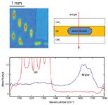
To capture the spectrum of water more clearly in the segment, imaging in transmission mode needs to be used. Figure 4 shows the image, the schematic diagram, and the extracted spectra of a water droplet flowing in oil in a wax-printed microfluidic device with a pathlength of 25 μm. The absorbance of water is far more pronounced compared to the spectrum extracted from the ATR measurement shown in Figure 3. However, as discussed in the transmission mode section, the large pathlength could lead to some parts of the spectral region becoming inaccessible. In this case, the spectral region in which oil absorbs IR light strongly (1100–1350 cm-1 ) is not accessible in the oil-rich region of the image. This is in contrast to the spectra extracted from the ATR imaging measurement, in which the absorbance of all spectral bands was less than 0.8, the value below which analysis can be quantitative. On the other hand, a large amount of the spectral range remains accessible in the water droplet region (1600–1000 cm-1). We have demonstrated previously that, despite the use of only one scan per image, the presence of protein can be detected at the ~1 mM level in the water segment in transmission mode by observing the amide II band at 1560 cm-1 (36).
Reactions
One of the potential benefits of combining FT-IR imaging with microfluidics is the in situ study of chemical reactions inside the channel. This allows for optimization of reaction conditions to obtain better yields, or understanding the diffusion and reaction kinetics inside the microfliudic device. This technique can be developed into a tool for chemical detection in microreactors for studying the effect of changing parameters to the overall efficiency. One of the examples (25) that demonstrated this potential was the observation of isotopic exchange between water and D2O forming HDO (semiheavy water). The spectral bands of H2O, D2O, and HDO are readily distinguishable. Because FT-IR measurements can be quantified, the concentrations of reactants and products at different points of the devices can be obtained. Another possible experiment is a reaction in a two-phase system in which one of the reactants is dissolved in the oil phase while the other reactant is dissolved in aqueous phase (37). The resultant effect is that the reaction can only happen at the interface between the two fluids. Diffusion profiles and the formation of product in such systems can be monitored simultaneously using the FT-IR imaging approach (37). This detection approach is set to benefit automation of reactions and other processes in microreactors (38).
Conclusions
In this article, we have discussed a methodology that permits the in situ chemical imaging of flows in microfluidic channels using FT-IR spectroscopic imaging that does not require added labels or dyes. This inherent chemical specificity of FT-IR imaging significantly adds to the detection capabilities of flows in microfluidic devices because it obtains quantitative chemical information as a function of space and time. This chemical imaging methodology has wide applicability to the study of dynamic systems ranging from the analysis and modeling of mixing in laminar flows to studies of reactions in segmented flows and separating live cells in moving droplets. We hope that this article can stimulate further applications of FT-IR spectroscopic imaging to study processes and reactions in microfabricated devices and microreactors because this methodology has great potential for in situ fast chemical analysis of microfluidic flows.
Acknowledgment
SGK acknowledges research funding from the European Research Council under the European Community's Seventh Framework Programme (FP7/2007-2013)/ERC advanced grant agreement no. [227950].
Dr. Ka Lung Andrew Chan is a Research Associate and Sergei G. Kazarian is a Professor of Physical Chemistry with the Department of Chemical Engineering at Imperial College London in London, UK. Please direct correspondence to: s.kazarian@imperial.ac.uk.
References
(1) A. Huebner, S. Sharma, M. Srisa-Art, F. Hollfelder, J.B. Edel, and A.J. Demello, Lab on a Chip 8, 1244 (2008).
(2) A.J. deMello, Nature 442(7101), 394 (2006).
(3) J. Aubin, M. Ferrando, and V. Jiricny, Chem. Eng. Sci. 65(6), 2065 (2010).
(4) N. Kockmann and D.M. Roberge, Chemical Engineering and Processing: Process Intensification 50, 1017 (2011).
(5) E.K. Hill and A.J. de Mello, Analyst 125(6), 1033 (2000).
(6) M. Lee, J.P. Lee, H. Rhee, J. Choo, Y.G. Chai, and E.K. Lee, J. Raman Spectrosc. 34(10), 737 (2003).
(7) J.B. Salmon, A. Ajdari, P. Tabeling, L. Servant, D. Talaga, and M. Joanicot, Appl. Phys. Lett. 86(9), 3 (2005).
(8) K.R. Strehle, D. Cialla, P. Rosch, T. Henkel, M. Kohler, and J. Popp, Anal. Chem. 79(4), 1542 (2007).
(9) A. Marz, T. Henkel, D. Cialla, M. Schmitt, and J. Popp, Lab on a Chip 11(21), 3584 (2011).
(10) G. Bergner, C.R. Albert, M. Schiller, G. Bringmann, T. Schirmeister, B. Dietzek, S. Niebling, S. Schlucker, and J. Popp, Analyst 136(18), 3686 (2011).
(11) S.G. Kazarian, Anal. Bioanal. Chem. 388(3), 529 (2007).
(12) J.L. Koenig and C.M. Snively, Spectroscopy 13(11), 22 (1998).
(13) C. Wagner, W. Buchegger, M. Vellekoop, M. Kraft, and B. Lendl, Anal. Bioanal. Chem. 400(8), 2487 (2011).
(14) E.N. Lewis, P.J. Treado, R.C. Reeder, G.M. Story, A.E. Dowrey, C. Marcott, and I.W. Levin, Anal. Chem. 67(19), 3377 (1995).
(15) C.M. Snively and J.L. Koenig, Macromolecules 31, 3753 (1998).
(16) S.G. Kazarian and K.L.A. Chan, Macromolecules 36, 9866 (2003).
(17) A. Gupper and S.G. Kazarian, Macromolecules 38 (6), 2327 (2005).
(18) K.L.A. Chan and S.G. Kazarian, Lab on a Chip 6(7), 864 (2006).
(19) S.G. Kazarian and K.L.A. Chan, Biochim. Biophys. Acta.-Biomem. 1758(7), 858 (2006).
(20) D. Velasco, C.B. Danoux, J.A. Redondo, C. Elvira, J. San Roman, P.S. Wray, and S.G. Kazarian, J. Contr. Release 149(2), 140 (2011).
(21) S.G. Kazarian and K.L.A. Chan, Appl. Spectrosc. 64(5), 135A (2010).
(22) K.L.A. Chan and S.G. Kazarian, J. Comb. Chem. 7(2), 185 (2005).
(23) K.L.A. Chan and S.G. Kazarian, J. Comb. Chem. 8, 26 (2006).
(24) C. Ricci, K.L.A. Chan, and S.G. Kazarian, Appl. Spectrosc. 60(9), 1013 (2006).
(25) K.L.A. Chan, S. Gulati, J.B. Edel, A.J. de Mello, and S.G. Kazarian, Lab on a Chip 9, 2909 (2009).
(26) T. Pan, R.T. Kelly, M.C. Asplund, and A.T. Woolley, in 26th International Symposium on Capillary Chromatography and Electrophoresis (Elsevier Science Bv, Las Vegas, Nevada, 2003), p. 231.
(27) J.C. McDonald, M.L. Chabinyc, S.J. Metallo, J.R. Anderson, A.D. Stroock, and G.M. Whitesides, Anal. Chem. 74(7), 1537 (2002).
(28) G.V. Kaigala, S. Ho, R. Penterman, and C.J. Backhouse, Lab on a Chip 7(3), 384 (2007).
(29) Y. Lu, W.W. Shi, L. Jiang, J.H. Qin, and B.C. Lin, Electrophoresis 30(9), 1497 (2009).
(30) E. Carrilho, A.W. Martinez, and G.M. Whitesides, Anal. Chem. 81(16), 7091 (2009).
(31) H.Y.N. Holman, R. Miles, Z. Hao, E. Wozei, L.M. Anderson, and H. Yang, Anal. Chem. 81(20), 8564 (2009).
(32) S.Y. Teh, R. Lin, L.H. Hung, and A.P. Lee, Lab on a Chip 8(2), 198 (2008).
(33) K.L.A. Chan, X. Niu, A.J. deMello, and S.G. Kazarian, Anal. Chem. 83(9), 3606 (2011).
(34) K. Ohta and R. Iwamoto, Appl. Spectrosc. 39(3), 418 (1985).
(35) K.L.A. Chan and S.G. Kazarian, Appl. Spectrosc. 61(1), 48 (2007).
(36) K.L.A. Chan, X.Z. Niu, A.J. de Mello, and S.G. Kazarian, Lab on a Chip 10(16), 2170 (2010).
(37) K.L.A. Chan and S.G. Kazarian, Anal. Chem. 84(9), 4052–4056 (2012).
(38) J.P. McMullen and K.F. Jensen, Annual Review of Analytical Chemistry, Vol 3, E.S. Yeung and R.N. Zare, Eds. (Annual Reviews, Palo Alto, California, 2010), p. 19.

AI Shakes Up Spectroscopy as New Tools Reveal the Secret Life of Molecules
April 14th 2025A leading-edge review led by researchers at Oak Ridge National Laboratory and MIT explores how artificial intelligence is revolutionizing the study of molecular vibrations and phonon dynamics. From infrared and Raman spectroscopy to neutron and X-ray scattering, AI is transforming how scientists interpret vibrational spectra and predict material behaviors.
Real-Time Battery Health Tracking Using Fiber-Optic Sensors
April 9th 2025A new study by researchers from Palo Alto Research Center (PARC, a Xerox Company) and LG Chem Power presents a novel method for real-time battery monitoring using embedded fiber-optic sensors. This approach enhances state-of-charge (SOC) and state-of-health (SOH) estimations, potentially improving the efficiency and lifespan of lithium-ion batteries in electric vehicles (xEVs).
New Study Provides Insights into Chiral Smectic Phases
March 31st 2025Researchers from the Institute of Nuclear Physics Polish Academy of Sciences have unveiled new insights into the molecular arrangement of the 7HH6 compound’s smectic phases using X-ray diffraction (XRD) and infrared (IR) spectroscopy.