3D Confocal Raman Imaging in Semiconductor Research
The exacting standards of quality and reliability of structured substrates in the semiconductor industry require in-depth knowledge concerning the interior structure of the devices. In this application note we present results of 3D confocal Raman imaging measurements for such characterizations.
Thomas Dieing, Marius Henrich1, and Eberhard Richter2, 1WITec GmbH, Ulm, Germany, and 2Ferdinand-Braun-Institute, Berlin, Germany
The exacting standards of quality and reliability of structured substrates in the semiconductor industry require in-depth knowledge concerning the interior structure of the devices. In this application note we present results of 3D confocal Raman imaging measurements for such characterizations.
Experimental Setup
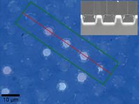
The sample used was a 20 μm thick GaN layer grown by a combination of HVPE and MOVPE on a patterned sapphire substrate at Ferdinand-Braun-Institute in Berlin. Figure 1 shows a top view of the holes overgrown by the GaN layer. Along the green rectangle a Raman XY and a Raman image stack scan series were performed. A depth profile was acquired along the red line. The insert shows a SEM image of a cross section of the sample's interior structure. The sample was examined using an alpha300 R+ confocal Raman microscope allowing high-resolution and high sensitivity 3D confocal Raman imaging.

Figure 1: Top view video image of the GaN layer. The area of the stack scans is shown in green and the red line shows the position of the depth scan. The insert shows a SEM cross section image of the patterned sapphire with the GaN layer on top.
Results
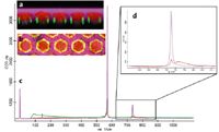
Figure 2 shows the spectral characteristics and the resulting images, revealing that in the depth-scan (a) three phases could be detected. The spectra (c + d) are displayed in corresponding colors.

Figure 2: Spectral characteristics of GaN layer with resulting images. (a) depth profile Raman image, (b) XY-scan Raman image, (c) + (d) corresponding Raman spectra.
In the magenta areas, the spectrum shows the typical features of GaN spectra. In the green area, which coincides with the edges of the holes, an enhanced fluorescence can be seen. This fluorescence is mainly located in the low-wavenumber range of the spectrum (green spectrum).
The red areas are located directly above the holes and spectrally show a strong reduction of the intensity of the A1 (LO) peak near 735 rel.1/cm but with an enhancement of a broad peak on the higher wavenumber side of this peak. This is shown in the zoomed view of the relevant spectral area (d). This peak shift and broadening suggests a more amorphous structure in this area.
Figure 2b shows one layer extracted from the stack scan. The typical spectral features are displayed using the same color code. It can be clearly seen that the fluorescence (green) is located at the outside walls of the holes and how the areas of the lower 735 rel.1/cm peak (red) are located on the inside of the holes.
Figure 3 shows a 3D Raman image reconstructed from the image stack data. The location of the fluorescence and the lower 735 rel.1/cm peak can be clearly identified at the positions of the hole.

Figure 3: 3D Raman image of the interior of the GaN layer.
Conclusion
3D confocal Raman imaging was used to investigate the properties of GaN grown on pattern sapphire. It was shown that an enhanced fluorescence signal can be detected at the perimeter of the etched structures and that the material directly above the holes in the structure showed a clearly modified Raman spectrum compared to bulk GaN.
WITec Instruments Corp.
122 McCammon Ave., Maryville, TN 37804
tel. (865) 984-4445, Fax: (865) 984-4441
Email: info@witec-instruments.com
Website: www.WITec-Instruments.com
