TMD Layer Characterization with Raman and RISE Microscopy


This study describes how Raman imaging and correlative Raman scanning electron (RISE) microscopy can characterize and visualize layer numbers in 2D MoS2 and WSe2 samples.
Transition metal dichalcogenides (TMDs) exhibit unique electronic and optical properties, and these differ depending on the number of layers of material. Raman imaging can quantify layers by these differences. Raman microscopy can also be combined with other techniques, such as scanning electron microscopy, for a more comprehensive view.
Experimental
An investigation of a tungsten diselenide flake quickly produced high-resolution images with a WITec alpha300 apyron fully automated Raman microscope.
Molybdenum disulfide monolayer crystals were examined with a WITec RISE system featuring a common vacuum chamber for both Raman and SEM measurements.
Results
Ultrafast Raman Analysis of Tungsten Diselenide (WSe2)
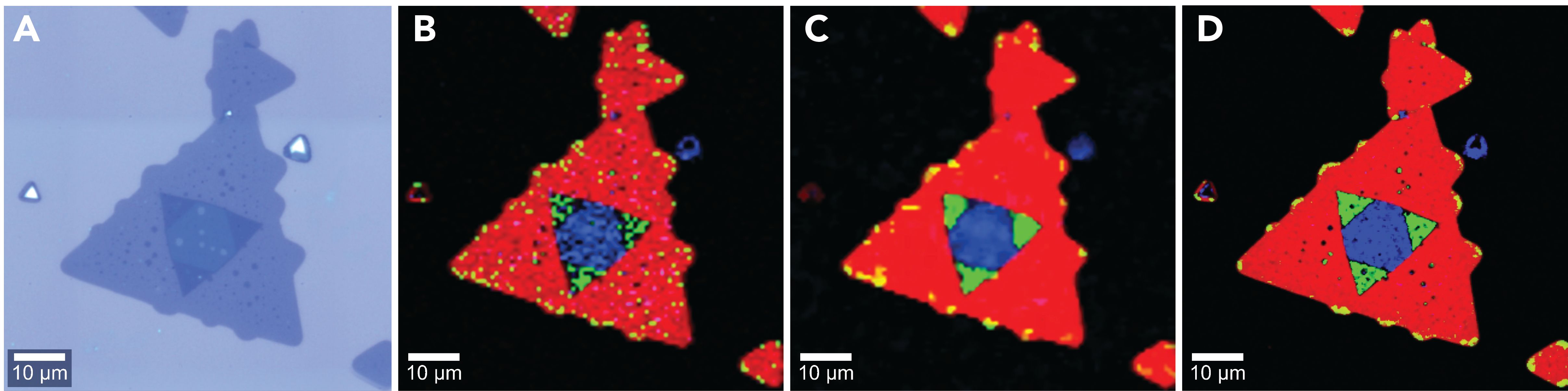
Figure 1B shows a measurement of a WSe2 flake that was acquired in approximately 2 min. It is a clear and detailed 75 × 75 µm² Raman image consisting of 10,000 spectra. The same data after smoothing are also shown. A measurement made in about 17 min of 100,000 spectra produced an even sharper image.

, bi-layer (green), multi-layer (blue).")
Figure 1: WSe2 flake A: White light image. B: Raman image of 10,000 spectra acquired in about 2 min. C: Smoothed version of B. D: Raman image of 102,400 spectra acquired in about 17 min. Color code: single-layer (red), bi-layer (green), multi-layer (blue).
RISE Microscopy Investigation of Molybdenum Disulfide (MoS2)
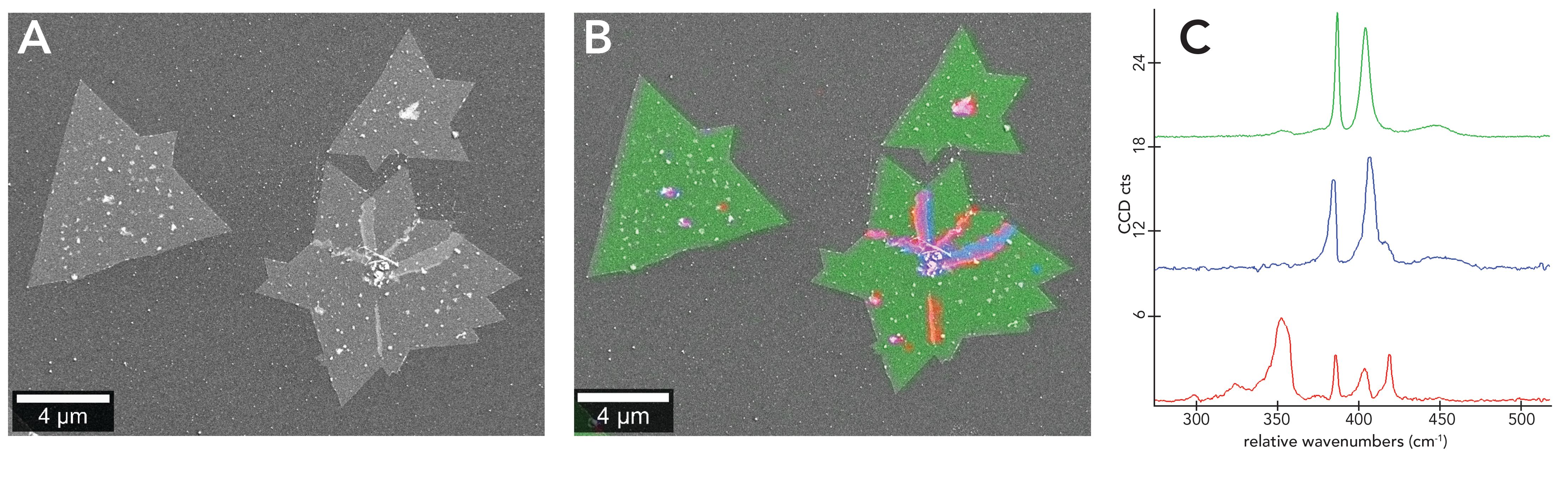
RISE microscopy reveals structure as well as crystalline and exciton dynamics of few-layered transition metal dichalcogenides (TMDs). Twin crystals of MoS2 on SiO2/Si appear in the SEM image as star-shaped forms (Figure 2A). The Raman spectra of MoS2 monolayers show the characteristic E’/E2g and A’1/A1g Raman band modes of MoS2 at 385 and 403 relative wavenumbers (cm-1) respectively (Figure 2C). With an increasing number of layers, the two Raman bands drift apart due to in-plane and out-of-plane (inter-layer) vibrations.
The grain boundaries visible in the SEM image correlate with the areas where Raman signals indicate crumpled or overlapping edges, highlighting the effectiveness of RISE microscopy (Figure 2B) for characterizing MoS2 crystals.

")
Figure 2: MoS2 crystals A: SEM image of MoS2 crystals. B: Color-coded Raman image derived from the spectral information overlaid on the SEM image to produce the RISE image. C: Raman spectra of MoS2: green = 1L MoS2, blue and red = edges and defects.
(Sample courtesy of Ting Yu, Nanyang Technological University, Singapore.)
Conclusion
Raman microscopy and the combination of Raman imaging with scanning electron microscopy offer researchers fast and versatile tools for determining the number of layers in transition metal dichalcogenide samples. High-resolution images of tungsten diselenide and molybdenum disulfide crystals can show edges, boundaries, folds, wrinkles, and other structures in clear, precise detail. This capability will be of great use as 2D materials and TMD research continues.
WITec GmbH
Lise-Meitner-Str. 6, 89081 Ulm, Germany
tel. +49 731 140 70 0, fax +49 731 140 70 200
Website: www.witec.de


New Study Reveals Insights into Phenol’s Behavior in Ice
April 16th 2025A new study published in Spectrochimica Acta Part A by Dominik Heger and colleagues at Masaryk University reveals that phenol's photophysical properties change significantly when frozen, potentially enabling its breakdown by sunlight in icy environments.


Advanced Raman Spectroscopy Method Boosts Precision in Drug Component Detection
April 7th 2025Researchers in China have developed a rapid, non-destructive Raman spectroscopy method that accurately detects active components in complex drug formulations by combining advanced algorithms to eliminate noise and fluorescence interference.


