SEIRAS-optimized ATR Wafers for Interfacial Spectroelectrochemistry
Special Issues
We show that a microgrooved ATR-SEIRAS optimized Si ATR wafer designed to allow high angles of incidence at the electrode-solution interface provides improved signal-to-noise in electrochemical ATR-SEIRAS.
We show that a microgrooved ATR-SEIRAS optimized Si ATR wafer designed to allow high angles of incidence at the electrode-solution interface provides improved signal-to-noise in electrochemical ATR-SEIRAS.
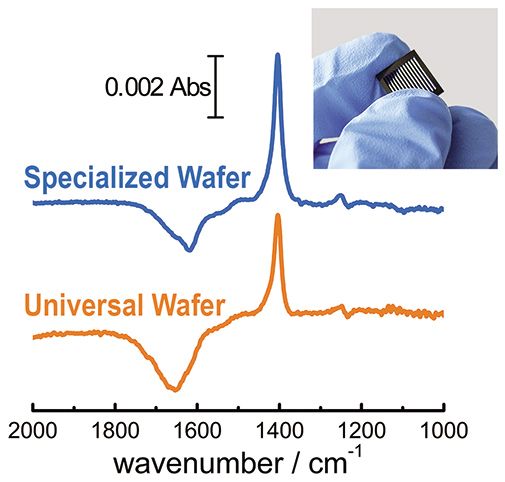
Microgrooved Si ATR wafers (Figure 2 inset) are excellent internal reflection elements for electrochemical ATR-SEIRAS owing to their low cost and high spectral throughput (1). A microgrooved substrate is formed by selective etching of a standard Si wafer to form an array of individual prisms. In this application note, the spectroelectrochemical performance of a specialized SEIRAS-optimized ATR wafer, with a grooved face angle (GFA) of 55°, was compared to a universal Si wafer ATR element (GFA of 35°).
Experimental Conditions
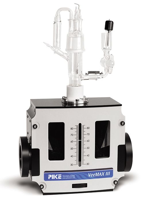
Identical 30 nm Au films, which serve as the working electrode in an ATR spectroelectrochemistry (SEC) cell, were sputtered on each wafer element (IRUBIS GmbH; Figure 2 inset). The wafer was loaded into a Jackfish J1W SEC Cell designed to interface with Si ATR wafers, and mounted on a VeeMAX III variable angle ATR accessory (PIKE Technologies; Figure 1). A Au coil counter electrode and a Ag/AgCl (saturated KCl) reference electrode were used. The cell was filled with 0.1 M pH 6 acetate buffer, and the Au thin film working electrode was activated by voltammetric cycling (2). FT-IR sample (E = +0.6 V, acetate adsorbed) and reference (E = -0.1 V, no adsorbed acetate) spectra were collected by coadding 128 scans at 4 cm-1 resolution, and potential difference absorbance spectra were calculated.

Figure 1: Jackfish J1W SEC Cell mounted on a VeeMAX III variable angle ATR accessory from PIKE Technologies.
Results
The angle of incidence (AOI) was varied between 30 to 65 ° to determine optimal response. This range is compressed by refraction to a narrow range at the electrode-solution interface defined by the GFA. For the specialized wafer, the optimal angle at the electrode-solution interface for maximum signal to noise (SNR) was near 50 °, and for the universal wafer it was 40 ° as determined by the acetate vCOO- band strength. Figure 2 shows the potential difference absorbance spectra at peak SNR for the specialized and universal crystals. The upward going band at 1400 cm-1 is the acetate vCOO- stretch. The weak band near 1200 cm-1 is due to potential dependent Si phonon modes. The broad negative band near 1650 cm-1 is due to loss of adsorbed interfacial water upon replacement with acetate. Both the higher signal and lower noise of the vCOO- stretch at 1400 cm-1 are apparent in the specialized spectrum.

Figure 2: The potential difference absorbance spectra of adsorbed acetate at peak SNR for specialized and universal wafers. Inset: microgrooved wafer ATR element.
Conclusions
The higher throughput and greater accessible AOI at the electrode-solution interface allows the specialized ATR-SEIRAS wafer to achieve a 35% greater SNR than that of the universal wafer in an electrochemical ATR-SEIRAS experiment.
References
(1) T.A. Morhart, B. Unni, M.J. Lardner, and I. Burgess, J. Anal. Chem. 89(21), 11818–11824 (2017).
(2) PIKE Technologies. Jackfish Spectroelectrochemistry Cells for Surface-Sensitive Electrochemical ATR-SEIRAS. Retrieved from https://www.piketech.com/Jackfish-SEC-Spectoelectrochemical-Cell.html.

PIKE Technologies, Inc.
6125 Cottonwood Drive, Madison, WI 53719
tel. (608) 274-2721, fax (608) 274-2721
Website: www.piketech.com

Chinese Researchers Develop Dual-Channel Probe for Biothiol Detection
April 28th 2025Researchers at Qiqihar Medical University have developed a dual-channel fluorescent probe, PYL-NBD, that enables highly sensitive, rapid, and selective detection of biothiols in food, pharmaceuticals, and living organisms.
New Study Reveals Insights into Phenol’s Behavior in Ice
April 16th 2025A new study published in Spectrochimica Acta Part A by Dominik Heger and colleagues at Masaryk University reveals that phenol's photophysical properties change significantly when frozen, potentially enabling its breakdown by sunlight in icy environments.
Advanced Raman Spectroscopy Method Boosts Precision in Drug Component Detection
April 7th 2025Researchers in China have developed a rapid, non-destructive Raman spectroscopy method that accurately detects active components in complex drug formulations by combining advanced algorithms to eliminate noise and fluorescence interference.

.png&w=3840&q=75)

.png&w=3840&q=75)


.png&w=3840&q=75)


.png&w=3840&q=75)


