Tech Note: Diffractive MEMS in Spectroscopy
Spectroscopy
MEMS are small, microfabricated devices that are finding application in a variety of industries in both analytical and manufacturing settings. This paper reviews the properties of diffractive MEMS devices and examines their application in chemical spectroscopy.
MEMS are small, microfabricated devices that are finding application in a variety of industries in both analytical and manufacturing settings. This paper reviews the properties of diffractive MEMS devices and examines their application in chemical spectroscopy.
The MEMS acronym, short for micro-electro-mechanical systems, evokes a vision of tiny machines (microsystems) that move. Indeed, a breathtaking array of microfabricated devices already is available commercially, and many more products are in various stages of development. What is common to the various MEMS devices is that, while being fabricated using tools commonly associated with the microelectronics industry, they all have some nonelectronic function, either in measurement, actuation, or display (1). This paper reviews the properties of diffractive MEMS devices and examines their application in chemical spectroscopy.

Electrically Programmable Diffraction
It is well known that a periodic array of lines or ridges formed on an otherwise flat surface will diffract light, splitting white light into its color constituents. What is less well known is that, using MEMS microfabrication techniques, it is possible to fabricate diffraction engines that have moving parts. David Bloom's group at Stanford University (Stanford, CA) has demonstrated a grating light valve device (2) in which groups of mechanical elements could be actuated together to create a diffracting "pixel." With such a device, it is possible to create electrically controllable diffraction patterns in which the diffracted light from an array of pixels can be projected to form an image. This capability has been commercialized by Silicon Light Machines (Sunnyvale, CA) for use in projection displays and also has been suggested for high-resolution printing applications (3). A variant of the original Bloom device was developed by Sandia National Laboratories (Livermore, CA) and tweaked by Polychromix (Wilmington, MA) to create synthetic chemical spectra using an array of individually controllable diffraction elements (4-6).
Spectroscopic Techniques
There are many ways to perform spectroscopy;
dispersive methods
, such as a scanned-grating monochromator or an optical multichannel analyzer (OMA) using a detector array, and
nondispersive methods
, such as an array or sequence of fixed filters, or Fourier transform spectroscopy using an interferometer with a moving mirror together with a fast Fourier transform algorithm. Each of these techniques provides different combinations of resolution, speed, sensitivity, and cost. In the visible part of the spectrum the development of the "video" chip has made diode-array technology widespread and inexpensive providing the market with many low cost OMA spectrometers (7). The "video" chip, nevertheless, is a silicon-based technology and therefore limited in the wavelength range it is responsive to, making it unusable at wavelengths longer than about 1 μm. While near-infrared diode arrays that function beyond one micron can be made using InGaAs, PbSe, and other semiconductors, this technology is less mature and can result in expensive devices. Thus, the OMA type of instrument has not had the same cost impact in the infrared, where the predominant chemical signatures exist, as it has in the visible part of the spectrum.
Throughput
The major advantage of OMAs is throughput; they measure all of the wavelengths all of the time. In contrast, a scanned-grating monochromator looks at only one wavelength at a time. The increased throughput of the OMA translates directly into improved signal-to-noise ratio. An alternate approach is the use of spectral encoding methods which can use up to half the wavelengths all of the time. This technique permits high-throughput spectrometers to be built with a single detector, as opposed to the more expensive detector arrays. A prime example of this is Fourier-transform IR (FT-IR) (8). FT-IR uses an interferometer with a moving mirror that encodes each wavelength into a different-frequency sinusoidal variation of intensity at the detector. All wavelengths are processed at the same time, resulting in an "interferogram." The resulting interferogram must then be deconvolved using a fast Fourier-transform algorithm. While these instruments have excellent performance characteristics and stability, to the point where FT-IR instruments are the
de facto
laboratory standard, they tend to occupy the higher-price portion of the spectrometer market. Low-cost spectrometers with high throughput can be built using alternative encoding techniques, as discussed below.
Encoding with Spatial Light Modulators
Other forms of encoding to create high-throughput single-detector spectrometers have been both proposed and demonstrated in the laboratory (9). These approaches all require a time-variable spectral filter to perform the encoding. One method of achieving this function is to disperse the light using a conventional fixed grating and image the spectrum on a spatial light modulator (SLM). An SLM is a device that controls the transmission or reflection of light electronically as a function of position on the SLM (9). Common examples are the liquid crystal display used on personal digital assistants, computer screens, and flat panel televisions. The SLM can be manipulated electronically to produce the spectral encoding sequence desired. A patent has been issued for a spectrometer based upon SLM technology (10). Liquid crystal technology is the most common for SLMs but it is limited spectrally by the nature of the materials used. Another approach to making an SLM uses diffractive MEMS, as discussed below.
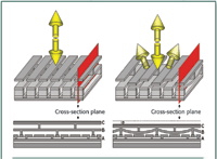
Figure 1. Schematic representation of diffractive MEMS structure: left - unactuated; right - actuated
A Diffractive SLM
Figure 1 shows a schematic of a section of the Polychromix diffractive MEMS chip, configured to function as an SLM. Figure 2 shows two microphotographs of a section of a prototypical chip (5). The chip contains an array of flat parallel mirror elements suspended on a structure that, when actuated, bends and lowers the mirror elements. In the unactuated state, light impinging at normal incidence simply is reflected back. However, when alternate beams are displaced, as in the right-hand side of Figure 1, the device becomes an efficient diffractor of light, with correspondingly less light returned by reflection along the original incident direction. Thus diffractive MEMS can be used as an effective spatial light modulator. When the displacement is exactly one-quarter of the wavelength of the incident light, there is ideally no light reflected back; all the light is diffracted.

Figure 2. Microphotographs of a diffractive MEMS chip illustrating the double-layer actuation scheme (from reference 5).
A unique feature of this approach is that because of the double-layer structure, the actuated reflector surface remains flat and parallel to the substrate. The diffraction phenomenon depends upon the respective difference in phase of the light reflected from the displaced and nondisplaced mirror elements. A flat displaced mirror element will have uniform phase across its entire surface, thus providing a more nearly ideal extinction of the reflected light under quarter-wavelength actuation. By controlling the deflection of these beams across the whole chip, an effective, reflective spatial light modulator can be achieved.
The diffractive MEMS spatial light modulator offers some advantages over other technologies such as liquid crystal. Because it is a reflective device, it can be used over a wide spectral range without regard to the optical transmission properties. Diffractive MEMS devices have resonant frequencies of 100 kHz or higher, resulting in an extremely rugged device that can survive shocks of greater than 20,000 g.
Digital Transform Spectroscopy
A particularly interesting method for digital spectral encoding is the Hadamard transform (11). This is a pseudorandom binary code that is all +1's and –1's. Such a transform matrix is shown in Figure 3. The horizontal axis is wavelength; the vertical axis is an integer that identifies the row of the matrix. Each row of dots represents one element of the digital transform, where a solid dot represents +1 and a white dot represents –1. In use, each row of the matrix is used sequentially. The SLM is set such that the light hitting each pixel is weighted either by +1 or –1, and the resulting intensity is summed at the detector. This gives one point in the transform spectrum. By executing a succession of such weightings, one for each row of the matrix, a time signal is produced as indicated by the "transform" graph to the right of the digital transform matrix. Computing the inverse digital transform from the resulting data yields the spectrum as a function of wavelength, as shown below the transform matrix.
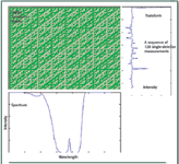
Figure 3. 128 x 128 digital transform matrix, illustrating the transform of the spectrum to the right and the recovered spectrum below.
The advantages of such a transform spectrometer in the IR are good throughput — it measures half of the wavelengths all of the time — and its use of a single detector element instead of a diode array, resulting in significant cost savings. Furthermore, the individual control of spectral elements offers the opportunity to fine-tune the measurement process. For example, spectral regions that are not of interest can be removed from the measurement process, improving signal-to-noise ratios and measurement times. Resolution is limited by the number of control elements of the spatial light modulator, implying that this technology will work better for liquids and solids, where broad spectral features are expected, rather than for gas spectra with very fine line structure, as can be seen in Figures 4 and 5.
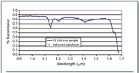
Figure 4. Sample scan of polystyrene using a Polychromix SLM device.
Programmable Operation Modes
Instead of using the aforementioned digital transform method, a scanning slit configuration can be programmed effectively in the MEMS chip by actuating in succession one pixel at a time. Another configuration mode replaces factory-fixed filter wheel spectrometers with MEMS-based on-the-fly software-programmable filter masks for the quick and efficient identification of a predefined, but possibly changing set of specimens. Analog weighting of each pixel can be achieved by using a non-binary transform that constitutes analog coefficients (not only ±1 values but also intermediate values). The ability to weight the intensity of different parts of the spectrum before summing on the single detector enables the development of a real-time form of chemometric analysis (12).
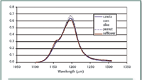
Figure 5. Absorbance spectra of five different household cooking oils.
References
1. S.D. Senturia,
Microsystem Design
(Kluwer Academic Publishers, 2001).
2. O. Solgaard, F.S.A Sandejas, and D.M. Bloom, Optics Letters17, 688-690 (1992).
4. M.B. Sinclair, M.A. Butler, A.J. Ricco, and S.D. Senturia, Applied Optics36, 3342-3348 (1997).
5. G.B. Hocker, D. Youngner, E. Deutsch, A. Volpicelli, S. Senturia, M. Butler, M. Sinclair, T. Plowman, and A.J. Ricco, "The Polychromator: A Programmable MEMS Diffraction Grating for Synthetic Spectra," Proc. Solid-State Sensor and Actuator Workshop (Hilton Head, SC, June 4-8, 2000), pp. 89-92.
6. M.B. Sinclair and K.B. Pfeifer, "Chemical sensing with a MEMS-based correlation radiometer," Materials Research Society Spring Meeting, San Francisco, CA; Symposium on Materials, Mechanisms and Systems for Chemical and Biological Detection and Remediation, April 14-15, 2004, paper Y4.1.
7. For example, see: www.oceanoptics.com
8. For example, see: www.scienceofspectroscopy.info
9. Robert Monteverde, "Spatial light modulators illuminate a wide variety of application spaces," Laser Focus World 41(1) 2004.
10. SLM Spectrometer US#5,504,575 Ronald E. Stafford Apr. 2, 1996.
11. Martin Harwit and Neil J.A. Sloane Hadamard Transform Optics, Chapter 2 (Academic, New York: 1979).
12. M. Otto, Chemometrics (Meinheim: Wiley-VCH, 1999).
M.A. Butler is vice president of research and development, Stephen Senturia is chief technology officer, and Yariv Geller is director of business development for Polychromix (Wilmington, MA). E-mail: ygeller@polychromix.com.

High-Speed Laser MS for Precise, Prep-Free Environmental Particle Tracking
April 21st 2025Scientists at Oak Ridge National Laboratory have demonstrated that a fast, laser-based mass spectrometry method—LA-ICP-TOF-MS—can accurately detect and identify airborne environmental particles, including toxic metal particles like ruthenium, without the need for complex sample preparation. The work offers a breakthrough in rapid, high-resolution analysis of environmental pollutants.
The Fundamental Role of Advanced Hyphenated Techniques in Lithium-Ion Battery Research
December 4th 2024Spectroscopy spoke with Uwe Karst, a full professor at the University of Münster in the Institute of Inorganic and Analytical Chemistry, to discuss his research on hyphenated analytical techniques in battery research.
Mass Spectrometry for Forensic Analysis: An Interview with Glen Jackson
November 27th 2024As part of “The Future of Forensic Analysis” content series, Spectroscopy sat down with Glen P. Jackson of West Virginia University to talk about the historical development of mass spectrometry in forensic analysis.
Detecting Cancer Biomarkers in Canines: An Interview with Landulfo Silveira Jr.
November 5th 2024Spectroscopy sat down with Landulfo Silveira Jr. of Universidade Anhembi Morumbi-UAM and Center for Innovation, Technology and Education-CITÉ (São Paulo, Brazil) to talk about his team’s latest research using Raman spectroscopy to detect biomarkers of cancer in canine sera.