Cryogenic Raman Imaging of a Tungsten Diselenide Flake
In a demonstration of the new cryoRaman low-temperature Raman microscope’s capabilities, a tungsten diselenide flake on Si/SiO2 was investigated and its numbers of layers were determined.
Interest in Raman microscopy at cryogenic temperatures has been increasing across a range of scientific fields over the past two decades. Though initially the primary driver of applications was the carbon nanotubes and graphene community, a recent surge in the number of published cryogenic Raman studies is dominated by research on transition metal dichalcogenides and van der Waals heterostructures.
To meet both existing and evolving market requirements, cryoRaman was jointly developed by cryogenic specialists attocube systems and Raman microscope developer WITec GmbH. It offers excitation wavelengths from vis to NIR with optimized spectrometers, 1.6 to 300 K operating temperatures, high magnetic fields, unique cryogenically compatible Raman-specific objectives, and an exceptionally precise piezoelectric scan stage.
In the following demonstration, cryoRaman was used to investigate a WSe2 flake on Si/SiO2, characterize its numbers of layers, and to establish the system’s sub-400 nm lateral resolution (1).
Experimental Conditions
To measure the tungsten diselenide flake, a 532 nm laser was used for excitation, and a RayShield coupler allowed detection of Raman bands down to ~±10 1/cm. The experimental setup also included a UHTS300 spectrometer optimized for detection in the visible range with an 1800 g/mm grating and a back-illuminated CCD camera.
The cryostat cooled the sample to 120 K. An LT-APO 532-Raman objective with a numerical aperture of 0.82 and piezoelectric positioners controlled through the Control Five software were used. The acquired data set was evaluated with the Project Plus software package.
Results
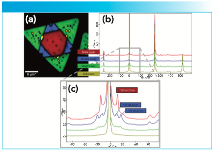
Images of the tungsten diselenide that show different numbers of layers were acquired and combined in the false color image shown in Figure 1a. It is color-coded according to the Raman spectra shown in Figure 1b. The image is 30 × 30 μm2 in size with 400 × 400 pixels and was created with an integration time of 150 ms per spectrum. A zoomed-in image (Figure 1c) shows the low-wavenumber area with the most prominent peaks for the double and triple layers as labelled.
Figure 1: Confocal Raman image of WSe2 of various layer numbers at 120K. (a) Combined false-color image showing the location of the different numbers of layers. (b) Raman spectra of the layers in the corresponding colors and (c) zoom-in of the spectra around the Rayleigh peak.

Conclusions
The cryoRaman microscopy system offers researchers a fast, user-friendly and versatile tool for examining transition metal dichalcogenide samples and determining their numbers of layers at very low temperatures. Its sub-400 nm lateral resolution together with low-wavenumber detection, high magnetic fields, and polarization control all make it unique in the marketplace. These capabilities will be of great use as research on 2D materials and TMDs continues.
Reference
(1) Extracted from the white paper: Cutting-edge Cryogenic Raman Microscope. https://www.witec.de/assets/Literature/Files/AppNote-cryoRaman.pdf
WITec GmbH
Lise-Meitner-Str. 6, 89081 Ulm, Germany
Tel. +49 (0) 731 140 700, Fax +49 (0) 731 140 70 200
Website: www.witec.de
