Raman and Phase Shifting Interferometry (PSI) Study of Tear/Fold Structure on Transferred Graphene

Graphene has been one of the most attractive materials in material engineering communities, due to its structure and high electron mobility. Its unique electronic band structure enables Raman spectroscopy to identify a single layer of graphene, and even to distinguish variable numbers of layers.
Combined with phase shifting interferometry (PSI), which investigates the height profile of 1 mm2 area in 0.5 nm resolution, Raman spectroscopy is a powerful method to analyze the morphology of not only two-dimensional graphene, but also transition of metal dichalcogenides. Those methods may be applied to quality control by detecting the defects, wrinkles, or torn parts of graphene sheets that can be generated from the transfer process during graphene fabrication.
Here, we observed the folded parts on a bilayer graphene sample with a Raman spectroscopy system, the XperRAM S Series, and with a PSI system, the Xper-PSI (both instruments manufactured by Nanobase, Inc.).
Materials and Methods
A layer sample of 1 cm2 of CVD graphene was fabricated by Graphene Supermarket. The graphene bilayer was transferred to 285 nm SiO2/Si (boron doped) substrate assisted by poly-methyl-methacrylate (PMMA) .
Raman spectra and Raman images were obtained with a Raman spectroscopy instrument, the XperRAM S Series. The Raman images were performed at those graphene’s intrinsic Raman peaks of G band (~1580 cm-1) and 2D band (~2700 cm-1). Averaging of spectra was performed from those parts where the silicon substrate is exposed and where the graphene layer is folded (2+2 tetralayer). The PSI images from the same parts were obtained via the Xper-PSI using
532 nm excitation.
Results and Conclusion
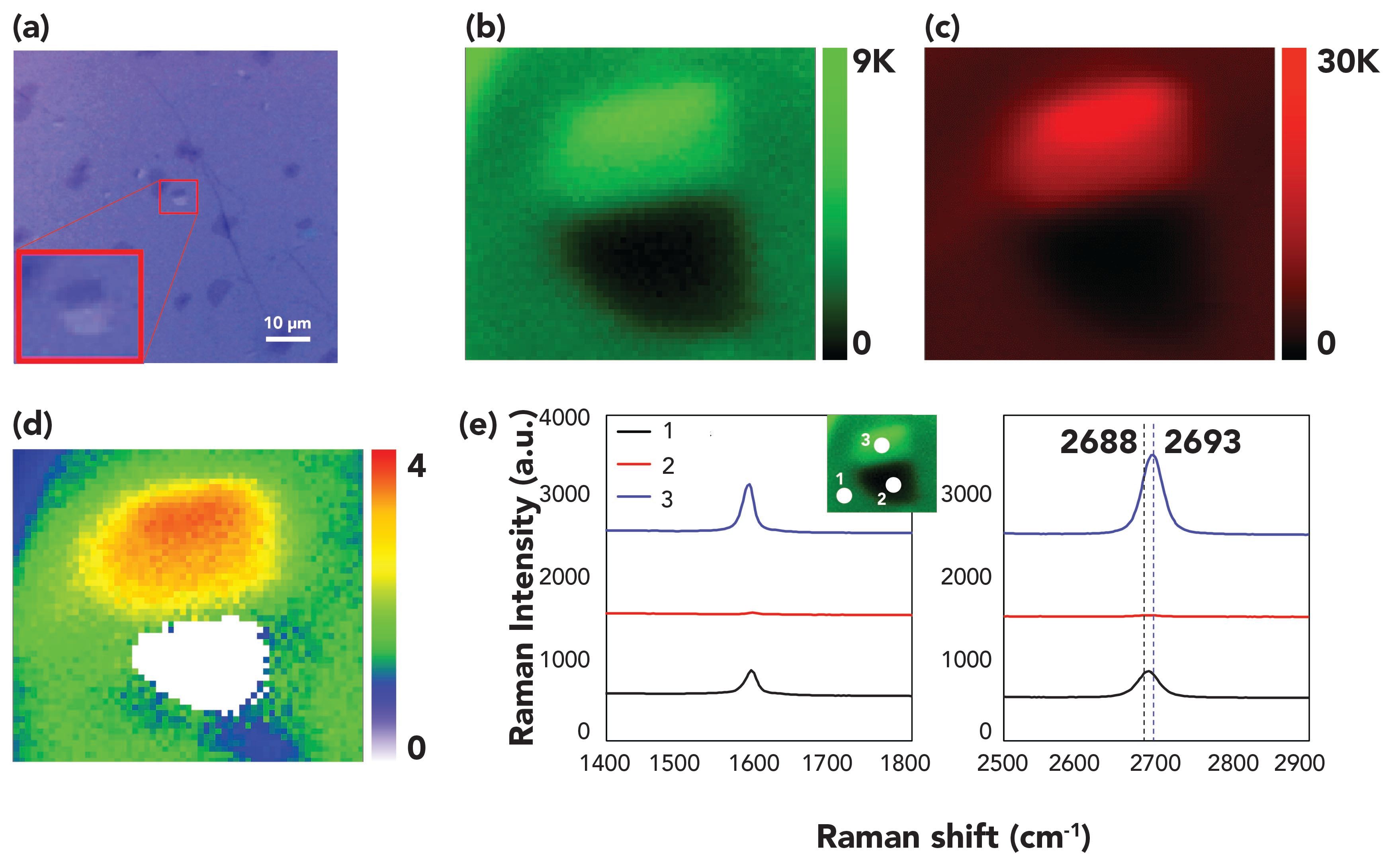
During the transfer of graphene on the growth substrate to the target substrate, sometimes a bit of the graphene area became torn and folded on the other side, symmetrically (1,2). This phenomenon was also found through a microscope (Figure 1a).
Figure 1: Optical image (a), Raman map (G (b), 2D (c) and 2D/G (d)) images, and Raman spectra of folded graphene (e)

Raman mapping was used to investigate the layer of graphene sheet and the properties of tear/fold structure (Figure 1 b–d). Through the 2D/G map (Figure 1d) and a spectrum at point 1 of Figure 1e, it was confirmed that bilayer graphene sheet was grown on the substrate. In Figure 1b and 1d, it was clearly seen that the two shapes were very similar. With the Raman map images of G and 2D bands and spectra of point 2 and 3 of Figure 1e, the direction of the graphene being folded was indicated.
In addition, by comparing spectra of specific areas from the Raman image in Figure 1e, intensity amplification of G, 2D band and the red shift (4~8 cm-1) again confirm the graphene tear and fold morphology (2).
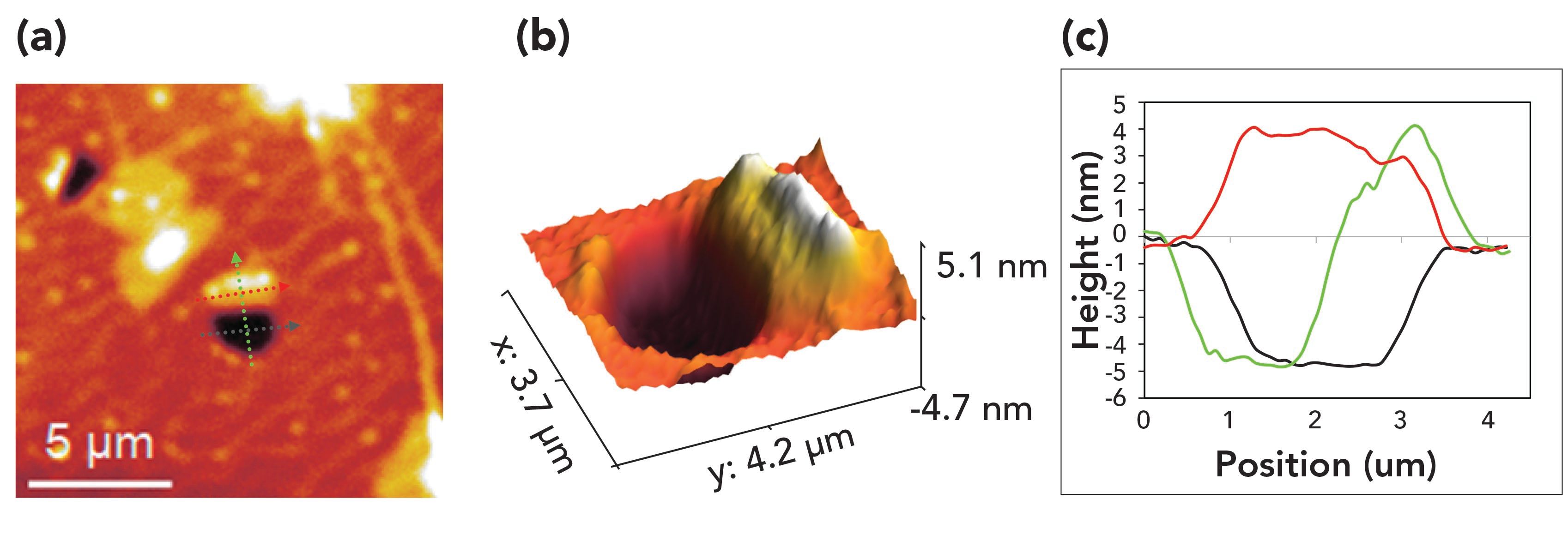
PSI was used to observe the profile of tear and fold area. The 2D PSI image and 3D-reconstructed images are shown in Figure 2a and 2b. Height profiles in Figure 2c prove that the depth between graphene sheet and substrate was about 4 nm, which was equal to the height of folded graphene sheets.
Figure 2: 2D (a) and 3D (b) phase shifting interferometry images and profiles of folded graphene (c).

Furthermore, the height of several torn or folded graphene sheets was examined, and bilayer graphene had 4 nm height.
Thus, supported by the PSI method, Raman spectroscopy has the capability to analyze the surface structure of nanomaterials, such as graphene, two-dimensional materials, nano-patterned surfaces, nanomaterials and so on.
References
U. Lee, et al., Adv. Mater., 2002854 (2020).
Y. Hao, et al. Small 6(2), 195–200 (2010).
Nanobase
1406-1, 196 Gasan-digital-1-ro, Geumcheon-gu,
Seoul 08502, South Korea
Tel. +82 70 8666 0233, Fax +82 2 852 9013
Website: www.nanobase.co.kr
