Raman Imaging of Silicon Structures
What exactly is a "Raman image" and how is it rendered? The authors explain those points, and demonstrate the use of Raman imaging for the characterization of thin-film and ion-implanted silicon structures. High spectral resolution makes it possible to resolve or contrast the substrate silicon and polysilicon film in Raman images and thus aids in the chemical or physical differentiation of spectrally similar materials.

Here we examine what is commonly called a Raman image and discuss how it is rendered. We consider a Raman image to be a rendering as a result of processing and interpreting the original hyperspectral data set. Building on the hyperspectral data rendering, we demonstrate the use of Raman imaging for the characterization of thin-film and ion-implanted silicon (Si) structures. A Raman image does not self-reveal solid-state structural effects and requires either the informed selection and assignation of the as-acquired hyperspectral data set by the spectroscopist or the use of statistical software applications. High spectral resolution allows us to clearly resolve the substrate Si Raman scattering from that of the polysilicon film. Consequently, high spectral resolution allows us to strongly resolve (structurally, not spatially) or contrast the substrate Si and polysilicon film in Raman images; that is, the spectral resolution contributes to the chemical or physical differentiation of spectrally similar materials in thin-film structures.
The primary goals of this column installment are to first examine in more detail what is commonly called a "Raman image" and to discuss how it is "rendered," and second to demonstrate the use of Raman imaging for the characterization of thin-film and ion-implanted silicon (Si) structures. The Raman images of Si and their rendering from the hyperspectral data sets presented here should encourage the reader to think more broadly of Raman imaging applications of semiconductors in electronic and other devices, such as microelectromechanical systems (MEMS). Raman imaging is particularly useful for revealing the spatial heterogeneity of solid-state structures in semiconductor devices. Here, test structures consisting of substrate silicon, silicon dioxide, polycrystalline silicon, and ion-implanted silicon are analyzed by Raman imaging to characterize the solid-state structure of the materials.
Before we begin our discussion on Raman imaging of silicon structures, we need to carefully consider and understand what actually constitutes a "Raman image." Consider the black and white photograph, perhaps the most basic type of image with which we are familiar. One can think of it as a three-coordinate system, with two spatial coordinates and one brightness (independent of wavelength) coordinate. Progressing to a color photograph, we now have a four-coordinate system by adding a chromaticity coordinate to the original three of a black and white image. That chromaticity coordinate in the color photograph is the key to thinking about hyperspectral imaging in general and Raman imaging in particular. Whether color discrimination is due to the cone cells in our eyes, the wavelength sensitive dyes in color photographic film, or the color filters fabricated onto charge-coupled device (CCD) sensors, a wavelength selection is imposed on the image. That color discrimination may not faithfully render a color image that corresponds to the true color of the object; for example, people who are color blind may not see the true colors of an object. In our daily lives, it is the combination of shape (two spatial coordinates), brightness (intensity coordinate), and color (chromaticity coordinate) that we interpret in the images we see to draw meaning and respond to the objects from which they originate. In that sense, image interpretation comes naturally to us and we begin to do it from a very early age without giving it much analytical thought.
When applying these same basic imaging principles of the four-coordinate system to hyperspectral imaging, the interpretation of the spectral (chromaticity) and intensity (brightness) coordinates are no longer "natural" and require mathematical thinking for proper interpretation. This mathematical thinking by the spectroscopist comes in the form of direct selection of spectral band position, width, shape, and resolution from closely spaced bands. The intensity coordinate is most often interpreted as the value at one particular peak or wavelength relative to that of another. However, even the simple application of an intensity coordinate requires the removal of background light unrelated to the spectroscopic phenomenon of interest. Furthermore, there are band-fitting operations and width and shape measurements that can be made and plotted against the two spatial coordinates to render an image. One can also apply any number of statistical and chemometric tools found in most scientific software. Therefore, whether the spectroscopist is directly engaged in the selection of spectral features and processing of the hyperspectral data set or simply uses statistical software operations, the spectral image is still the rendered product from a group of mathematical functions operating on the data.
Now let's apply these hyperspectral imaging considerations to Raman imaging. We are all too familiar with the fluorescent background that often accompanies Raman scattering. In some instances, the spectroscopist will digitally subtract the fluorescent background before rendering a spectrum that consists almost exclusively of Raman data. By analogy, we might expect the same practice to hold if we wish to call an image a "Raman image" rather than a "spectral image" (one that includes data from all light from the object). For example, if the signal strength in a hyperspectral image detected at a particular Raman shift consists of 90% fluorescence and only 10% Raman scattering, it would not be correct to call that a Raman image. However, if the fluorescent background and any contribution from a light source other than Raman scattering is first removed, then we have a Raman image. Having done that, we are not necessarily finished rendering our Raman image. If we wish to spatially assign chemical identity or another physical characteristic to the image, the data must be interpreted either through a spectroscopist's understanding of chemistry and physics or through the statistical treatment of the data. The spectral image data as acquired are not self-selecting or -interpreting. It is only after applying the spectroscopist's judgment or statistical tools that one renders a color coded Raman image of compound A, compound B, and so on.
I hope that you can see (pun intended) that Raman imaging is not an entirely simple matter or as intuitive as photography. Rather, it requires careful attention to the mathematical operation on the data and interpretation of the results. A Raman image is rendered as a result of processing and interpreting the original hyperspectral data set. The proper interpretation of the data to render a Raman image requires an understanding or at least some knowledge of the processes by which the image was generated.
Imaging Strain and Microcrystallinity in Polysilicon
The development of Raman spectroscopy for the characterization of semiconductors began in earnest in the mid-1970s, and micro-Raman methods for spatially resolved semiconductor analysis were being used in the early 1980s. An account of the work in those early years can be found in the excellent book by Perkowitz (1). Perhaps even more surprising to young readers is the fact that one can find the words "Raman image" in either the title or text of some of those 1980s publications (2–4). Much of that early work involved the development of micro-Raman spectroscopy for the characterization of polycrystalline silicon (5–8), also known as polysilicon, which is still used extensively in fabricated electronic devices. Theoretical and experimental work was directed toward an understanding of how strain, microcrystallinity, and crystal lattice defects or disorder can all affect the Raman band shape, position, and scattering strength of single and polycrystalline silicon (9–11). The presence of nanocrystalline Si in polysilicon was confirmed through the combination of transmission electron microscopy and Raman spectroscopy, and the effects of extremely small Si grain dimensions on the Raman spectra were attributed to phonon confinement (12–15). As the crystalline grain size becomes smaller, comparable to the wavelength of the incident laser light or less, the Raman band broadens and shifts relative to that obtained from a crystalline domain significantly larger than the excitation wavelength. This has been explained in part by phonon confinement in which the location of the phonon becomes more certain as the grain size becomes smaller, and therefore the energy of the phonon measured must become less certain, consistent with the Heisenberg uncertainty principle. Now, with all that as historical background, let's take a fresh look at the Raman imaging of Si structures with work done and Raman images rendered in the first months of 2013.
A collection of data from a polysilicon test structure is shown in Figure 1. A reflected white light image of the structure appears in the lower right-hand corner and a Raman image corresponding to the central structure in the reflected light image appears to its left. The plot on the upper left consists of all of the Raman spectra acquired over the image area and the upper right-hand plot is of the single spectrum associated with the cursor location in the Raman and reflected light images. The Raman data were acquired using 532-nm excitation and a 100× Olympus objective and by moving the stage in 200-nm increments over an approximate area of 25 μm × 25 μm. Now we make our first selection and operation on the hyperspectral data set. In this particular case, the Raman image is rendered through a color-coded plot of Raman signal strength over the corresponding color-bracketed Raman shift positions in the two upper traces.
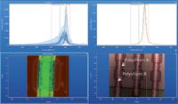
Figure 1: Raman hyperspectral data set from a polysilicon test structure with white reflected light image in lower right corner. The Raman image (lower left) corresponds to the color-coded bracketed regions in the spectral traces. The single spectrum (upper right) corresponds to the crosshairs in the Raman and white reflected light images.
Let's discuss the reasoning behind our choice of the brackets and how they relate to differences in the solid-state structure of Si. If we were to have a merely elemental compositional image of this particular structure, we would expect it to be entirely uniform without spatial variation because Si would appear in every pixel of the image. However, if we distinguish the different solid-state structures of the Si by identifying pristine Si with the Brillouin zone center Raman band of 520.7 cm-1 isolated in red brackets, microcrystalline and strained Si in green brackets, and a distribution of nanocrystallinity and strain in the blue brackets, we can render the Raman image in the lower left-hand corner. To some degree strain, microcrystallinity, and nanocrystallinity are commingled in the polysilicon regions of our images; however, we can make a crude distinction by attributing the blue regions as primarily a result of the nanocrystalline grain size.
Now let's take a close look at what our rendering reveals in our Raman image, expanded for more detailed examination in Figure 2. The red regions consist of either substrate Si or grown single-crystal Si with different oxide thicknesses. The spatial variation of the single-crystal Raman signal strengths corresponds precisely with the physical optical effects of the oxide thicknesses and even small contaminants or defects seen in the reflected light image. Furthermore, because of the thinness of the polysilicon A alone, one can see through the green polysilicon A component to the underlying red substrate Si, particularly on the left and right of the upper and lower portions of Figure 2. The spatial variation of the microcrystalline or strained Si green component signal strength corresponds to both the central strip consisting of polysilicon B deposited on polysilicon A and the granular variation of polysilicon A seen in the reflected light images. Note that the polysilicon A bright green speckles in the Raman image correspond precisely to black speckles in the reflected light image. Careful examination of the central strip reveals these same speckles in the polysilicon A blurred somewhat by the polysilicon B deposited on top of it.
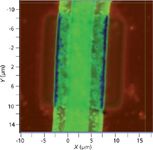
Figure 2: The Raman image from Figure 1. Red corresponds to single crystal silicon, green is the strained and microcrystalline polysilicon, and blue is the nanocrystalline silicon. Polysilicon B (in the center) was deposited on the wider, underlying polysilicon A.
Next let's turn our attention to the blue nanocrystalline portion of the image. The formation of nanocrystalline Si occurs almost exclusively in polysilicon A and only on top of the central single-crystal Si structure and not the substrate Si. Note that the nanocrystallinity occurs primarily along the edge of the polysilicon A, but disappears as the polysilicon A continues along the Si substrate. Also, we see that some of the polysilicon A speckles appear blue, thereby revealing nanocrystallinity over the central structure, but not over the Si substrate.
In summary, the intensity variations of the single-crystal Si comport with the physical optical effects of varying oxide film thickness and surface contaminants. Also, this Raman image reveals the spatially varying nanocrystallinity, microcrystallinity, and strain in polysilicon. We can infer that these structural differences occur either as a result of processing conditions or from interactions with the adjacent or underlying materials in which the polysilicon is in contact. This exercise clearly demonstrates that a Raman image does not self-reveal solid-state structural effects without the informed selection and assignation of the as acquired hyperspectral data set.
Imaging Crystal Lattice Damage Induced by Ion Implantation
Next, we examine the Raman imaging of that portion of our polysilicon test structure in which single-crystal silicon and polysilicon portions have been subjected to high energy ion implantation for the placement of dopants in the circuitry. The entire hyperspectral data set of one such region is shown in Figure 3. Again we have a structure consisting of Si substrate, isolated single-crystal Si, polysilicon A and B, silicon oxides, and a region implanted at high energy with As+. The Raman spectra were acquired over an area of approximately 30 μm × 30 μm using a 100× Olympus objective with 532-nm excitation and moving the electronically controlled stage in 200-nm increments.
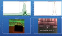
Figure 3: Raman hyperspectral data set from an ion-implanted polysilicon test structure with white reflected light image in the lower right corner. The Raman image (lower left) corresponds to the color-coded bracketed regions in the spectral traces. The single spectrum (upper right) corresponds to the lower left-hand corner of the Raman image. The ion-implanted Si yields only a weak Raman spectrum that resembles amorphous silicon, thereby appearing black in the Raman image. To get a better perspective on the importance of Raman imaging registration with the corresponding white light image see the YouTube video called "Raman Image Registration" (www.youtube.com/watch?v=rhHCOz-YEtc&feature=youtu.be).
High energy ion implants disrupt the crystal lattice to varying degrees depending on the atomic mass, dose, and kinetic energy of the implanted ions. In this case, the heavy arsenic ions have completely damaged the crystal lattice. The long-range translational symmetry of the Si has been disrupted such that the Raman scattering from the ion-implanted Si arises from phonons throughout the Brillouin zone and not just the Brillouin zone center as in crystals. Consequently, ion-implanted Si yields only a weak Raman spectrum that resembles amorphous silicon (16–20). For this reason, the implant appears dark in the Raman image. Note that ion implantation affects the reflectance of the Si and that is why the implanted regions appear lighter than the adjacent unimplanted Si in the white reflected light image. Therefore, we have a good way of confirming the accuracy of our Raman image rendering by its registration with the white reflected light image. To get a better perspective on the importance of Raman imaging registration with the corresponding white light image see the YouTube video called "Raman Image Registration" (www.youtube.com/watch?v=rhHCOz-YEtc&feature=youtu.be).
Let's more carefully examine the expanded Raman image of the implanted structure shown in Figure 4. The substrate and isolated single-crystal Si can be seen in the lower half of the image and can also be seen underneath the polysilicon structures in the upper half. The spatial variations of the red intensities correspond well to the edges and contaminants or defects in the white reflected light image. The ion-implanted region contrasts strongly with single-crystal Si and polysilicon because of the weakness of the Raman signal from implanted, amorphized Si in all three of the bracketed spectral regions. Single-crystal Si and the lower edge of polysilicon A have both been implanted and the Raman image reveals the damage to the crystal lattice of both forms of Si. Also, note the sharpness of the Raman image and its registration with the reflected light image, which reveal the efficacy of Raman imaging as a means for ion implant placement and registration. To get a better perspective on how ion implantation affects the Raman image and to view individual spectra in the implant region see the YouTube video called "Raman Imaging of Implanted Si and Polysilicon" (http://www.youtube.com/watch?v=Cf41DKhPzCs&feature=youtu.be).
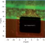
Figure 4: The Raman image from Figure 3. Red corresponds to single-crystal silicon, green corresponds to strained and microcrystalline polysilicon, and blue corresponds to nanocrystalline silicon. The ion-implanted Si yields only a weak Raman spectrum that resembles amorphous silicon, thereby appearing black in the Raman image. To get a better perspective on how ion implantation affects the Raman image and to view individual spectra in the implant region see the YouTube video called "Raman Imaging of Implanted Si and Polysilicon" (www.youtube.com/watch?v=Cf41DKhPzCs&feature=youtu.be).
The polysilicon portions of the structure reveal the bright speckles from the polysilicon A that directly correspond to each of the black speckles in the white light reflected image. In contrast to the Si structures shown in Figures 1 and 2, the processes or adjacent materials have not induced the same degree of nanocrystallinity in this location of polysilicon A. Here, again, we have a structure with both forms of polysilicon and isolated Si, but the edges induced only a small amount of nanocrystallinity as revealed by the light blue streak along the polysilicon edge. Also, we are again able to "see" through the polysilicon to the Si substrate or isolated single-crystal Si. Note that the low energy limit of the red bracket begins at 520 cm-1, and so the red region does reasonably differentiate substrate and isolated single-crystal Si from polysilicon. The Raman images in the next section allow us more insight into this effect.
Imaging and the Importance of Spectral Resolution
Now we address the importance of spectral resolution for the generation of Raman images of thin-film structures in general and diffusely reflecting Si-based electronic devices in particular. Figure 5 shows the hyperspectral data set, the white reflected light image, and the approximately 14 μm × 22 μm Raman image from that portion of the test structure that consists only of polysilicon A and B on substrate Si. The L-shaped region of the images consists of (from bottom to top) substrate Si, polysilicon A, and polysilicon B. Note that the Raman bands of the different forms of Si in the hyperspectral data set (upper left) are better resolved than those in Figures 1–4. This is entirely because of differences in the solid-state structure of the polysilicon because the same spectrometer, grating (1800 gr/mm), and microscope objective were used for all data acquisition reported here. Raman spectra consisting wholly of broad, low energy bands peaking between 490 and 510 cm-1 clearly reveal the presence of nanocrystallinity in the polysilicon.
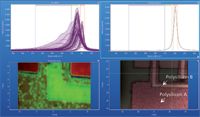
Figure 5: Raman hyperspectral data set from a polysilicon test structure with white reflected light image in lower right corner. The Raman image (lower left) corresponds to the color-coded bracketed regions in the spectral traces. The single spectrum (upper right) corresponds to the upper right-hand corner of the Raman image.
Let's more carefully examine the material contrast in the expanded Raman image of the polysilicon structure shown in Figure 6. As we saw in the previous Raman images, polysilicon A shows a far greater propensity for forming nanocrystalline Si at the edges and distributed in some of the speckle. Polysilicon B also shows some nanocrystallinity at the edges; however, it is to a far lesser degree than in polysilicon A. The increased thickness of polysilicon B on top of A accounts for the bright green signal in the L-shaped region and the very dim red contribution from the underlying Si substrate. In that region, with only one layer of polysilicon A covering the substrate Si, the underlying red single-crystal Si signal emerges strongly through that of the green polysilicon A. The high spectral resolution allows us to clearly resolve the single-crystal Si Raman bands in the red bracket from those of the polysilicon in the green bracket. Consequently, in this particular structure of only polysilicon on Si substrate, the high spectral resolution allows us to strongly resolve (structurally, not spatially) or contrast the substrate Si and polysilicon in Raman images; that is, the spectral resolution contributes to the chemical or physical differentiation of spectrally similar materials in thin-film structures.
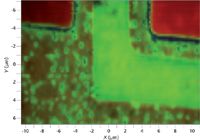
Figure 6: The Raman image from Figure 5. Red corresponds to substrate silicon, green corresponds to strained and microcrystalline polysilicon, and blue corresponds to nanocrystalline silicon.
Excitation wavelength also plays an important role in depth profiling semiconductor structures (19). An excitation wavelength shorter than 532 nm would have a shallower depth of penetration in Si (21), and so we might expect the Raman images generated using different excitation wavelengths to look different. At some shorter excitation wavelength, depending on the thickness of the polysilicon, one would no longer be able to detect the underlying Si substrate or single-crystal Si because of the shallow depth of penetration. We'll have to save Raman image depth profiling by excitation wavelength selection for another installment of "Molecular Spectroscopy Workbench."
Conclusions
We have examined in more detail what is commonly called a Raman image and discussed how it is rendered. We claim that a Raman image is rendered as a result of processing and interpreting the original hyperspectral data set. The proper interpretation of the data to render a Raman image requires an understanding or at least some knowledge of the processes by which the image was generated. Building on the hyperspectral data rendering, we demonstrate the use of Raman imaging for the characterization of thin-film and ion-implanted silicon structures. We show that a Raman image does not self-reveal solid-state structural effects, but requires either the informed selection and assignation of the as acquired hyperspectral data set by the spectroscopist or the use of statistical software applications. High spectral resolution allows us to clearly resolve the substrate Si Raman scattering from the polysilicon film. Consequently, high spectral resolution allows us to strongly resolve (structurally, not spatially) or contrast the substrate Si and polysilicon film in Raman images; that is, the spectral resolution contributes to the chemical or physical differentiation of spectrally similar materials in thin-film structures.
References
(1) S. Perkowitz, Optical Characterization of Semiconductors: Infrared, Raman, and Photoluminescence Spectroscopy (Academic Press, London, UK, 1993), Chap. 6.
(2) K. Mizoguchi, Y. Yamauchi, H. Harima, S. Nakashima, T. Ipposhi, and Y. Inoue, J. Appl. Phys. 78, 3357–3361 (1995).
(3) S. Nakashima, K. Mizoguchi, Y. Inoue, M. Miyauchi, A. Mitsuishi, T. Nishimura, and Y. Akasaka, Jpn. J. Appl. Phys. 25, L222–L224 (1986).
(4) K. Kitahara, A. Moritani, A. Hara, and M. Okabe, Jpn. J. Appl. Phys. 38, L1312–L1314 (1999).
(5) Y. Inoue, S. Nakashima, A. Mitsuishi, T. Nishimura, and Y. Akasaka, Jpn. J. Appl. Phys. 25, 798–801 (1986).
(6) D.R. Tallant, T.J. Headley, J.W. Medernach, and F. Geyling, Mat. Res. Soc. Symp. Proc. 324, 255–260 (1994).
(7) D.V. Murphy and S.R.J. Brueck, Mat. Res. Soc. Symp. Proc. 17, 81–94 (1983).
(8) G. Harbeke, L. Krausbauer, E.F. Steigmeier, A.E. Widmer, H.F. Kappert, and G. Neugebauer, Appl. Phys. Lett. 42, 249–251 (1983).
(9) G.-X. Cheng, H. Xia, K.-J. Chen, W. Zhang, and X.-K. Zhang, Phys. Stat. Sol. (a) 118, K51–K54 (1990).
(10) N. Ohtani and K. Kawamura, Solid State Commun. 75, 711–715 (1990).
(11) H. Richter, Z.P. Wang, and L. Ley, Solid State Commun. 39, 625–629 (1981).
(12) Z. Iqbal and S. Veprek, SPIE Proc. 794, 179–182 (1987).
(13) V.A. Volodin, M.D. Efremov, and V.A. Gritsenko, Solid State Phenom. 57–58, 501–506 (1997).
(14) Y. He, C. Yin, G. Cheng, L. Wang, X. Liu, and G.Y. Hu, J. Appl. Phys. 75, 797–803 (1994).
(15) H. Xia, Y.L. He, L.C. Wang, W. Zhang, X.N. Liu, X.K. Zhang, D. Feng, and H.E. Jackson, J. Appl. Phys. 78, 6705–6708 (1995).
(16) R. Tripathi, S. Kar, and H.D. Bist, J. Raman Spec. 24, 641–644 (1993).
(17) D. Kirillov, R.A. Powell, and D.T. Hodul, J. Appl. Phys. 58, 2174–2179 (1985).
(18) D.D. Tuschel, J.P. Lavine, and J.B. Russell, Mat. Res. Soc. Symp. Proc. 406, 549–554 (1996).
(19) D.D. Tuschel and J.P. Lavine, Mat. Res. Soc. Symp. Proc. 438, 143–148 (1997).
(20) J.P. Lavine and D.D. Tuschel, Mat. Res. Soc. Symp. Proc. 588, 149–154 (2000).
(21) Raman and Luminescence Spectroscopy of Microelectronics: Catalogue of Optical and Physical Parameters, "Nostradamus" Project SMT4-CT-95-2024 (European Commission, Science, Research and Development, Luxembourg, 1998), p. 20.
David Tuschel is a Raman applications manager at Horiba Scientific, in Edison, New Jersey, where he works with Fran Adar. David is sharing authorship of this column with Fran. He can be reached at: david.tuschel@horiba.com

David Tuschel

Ancient Meteorite Reveals Space Weathering Secrets Through Cutting-Edge Spectroscopy
Published: May 27th 2025 | Updated: May 27th 2025Researchers in Rome used advanced spectroscopic techniques to probe the mineralogy of the CM2 carbonaceous chondrite NWA 12184. This revealed the effects of space weathering and provided insights into C-type asteroid evolution.
Nanometer-Scale Studies Using Tip Enhanced Raman Spectroscopy
February 8th 2013Volker Deckert, the winner of the 2013 Charles Mann Award, is advancing the use of tip enhanced Raman spectroscopy (TERS) to push the lateral resolution of vibrational spectroscopy well below the Abbe limit, to achieve single-molecule sensitivity. Because the tip can be moved with sub-nanometer precision, structural information with unmatched spatial resolution can be achieved without the need of specific labels.
Multi-Analytical Study Reveals Complex History Behind Ancient Snake Motif in Argentine Rock Art
May 22nd 2025A recent study published in the Journal of Archaeological Science: Reports reveals that a multi-headed snake motif at Argentina's La Candelaria rock shelter was created through multiple painting events over time.

.png&w=3840&q=75)

.png&w=3840&q=75)


.png&w=3840&q=75)


.png&w=3840&q=75)


