Resonance Raman and Photoluminescence Spectroscopy and Imaging of Few-Layer MoS2
Resonance and off-resonance Raman spectroscopy and imaging are used to examine the spatial variation of the solid-state structure and electronic character of few-layer MoS2 flakes. Simultaneous acquisition of photoluminescence spectra with the Raman scattering provides complementary ways of rendering Raman and photoluminescence spectral images of thin-film MoS2.
Resonance and off-resonance Raman spectroscopy and imaging are used to examine the spatial variation of the solid-state structure and electronic character of few-layer MoS2 flakes. Simultaneous acquisition of photoluminescence spectra with the Raman scattering provides complementary ways of rendering Raman and photoluminescence spectral images of thin-film MoS2.
Graphene is probably the most well-known substance of the emerging class of materials known as two-dimensional (2D) crystals. These materials are constituted by monolayer and few-layered structures. In recent years, new inorganic 2D materials have emerged, including MoS2, MoSe2, WS2, and WSe2. These materials have attracted significant interest because of special electronic, optical, and optoelectronic properties in the monolayer and few-layer forms that are different from those manifested by the bulk form (1,2). One of the most significant differences of the 2D crystals is the transformation from an indirect band gap semiconductor in the bulk to a direct band gap semiconductor in the monolayer and few-layer crystals. Thus, the fabrication of optoelectronic devices in addition to familiar integrated electronic circuitry is envisioned for these materials. These optoelectronic characteristics have prompted substantial research to discover the means of fabrication and the physical characteristics of two-dimensional crystals to produce integrated electronic and optoelectronic devices (3).
Many articles on nanomaterials emphasize the means to fabricate the materials, their properties, and their performance when constructed as devices (4). However, there is a great need for characterization of these materials because of their experimental nature and structural variability, often within one film. After all, none of these materials are of the nature of a compound that can be taken out of a reagent bottle. Consequently, there have been attempts to develop analytical methods for the reliable characterization of 2D crystals. You may have observed the spatially varying colors in reflected white light images of nanomaterials, and so there have been developments to use optical microscopy to rapidly identify the number of molecular layers that make up the 2D crystal (5). In this installment, we focus on Raman and photoluminescence spectroscopy and imaging for the characterization of these experimental materials.
Two-dimensional crystals are not just small portions of the bulk materials carrying the same properties as those of the three-dimensional kind. Rather, their physical, electronic, and spectral characteristics can be significantly different. Specifically, MoS2 in its bulk form is an indirect bandgap semiconductor, whereas in its monolayer and few-layer forms it becomes a direct bandgap semiconductor (6). Splendani and coworkers (7) studied exfoliated MoS2 monolayer and few-layer flakes by photoluminescence and observed direct excitonic transitions. Exciting with 532-nm laser light they observed broad photoluminescence centered at 627 and 677 nm, whereas these emissions are completely absent when illuminating bulk MoS2. The room-temperature bandgap of bulk MoS2 is approximately 1.7 eV (corresponding to 730 nm) with complex excitonic features between 1.7 and 2.5 eV (8).
The crystalline structure of 2H-MoS2 belongs to the D6h crystal class, and factor group analysis predicts one A1g, one E1g, and two E2g Raman active modes (8–14). The symmetry assignments and corresponding Raman band positions for bulk hexagonal MoS2 are as follows: E1g (286 cm-1), E12g (383 cm-1), A1g (408 cm-1), and E22g (32 cm-1). Furthermore, it is important to remember that some visible wavelengths of the laser light used to excite Raman scattering correspond to energies of MoS2 electronic transitions. The absorption spectrum of MoS2 reflects the band gap of 1.7 eV, but it also manifests fine structure with narrow absorption peaks at 1.9 eV (653 nm) and 2.1 eV (590 nm) related to d-to-d orbital transitions split by spin-orbit coupling and designated A1 and B1 excitons, respectively (8,15). Consequently, one can observe an excitation wavelength dependence of the first-order Raman band intensities as well as the appearance of Raman bands assigned to harmonic and combination modes when the laser excitation is of a wavelength that couples into these excitonic transitions (8,12,14,15).
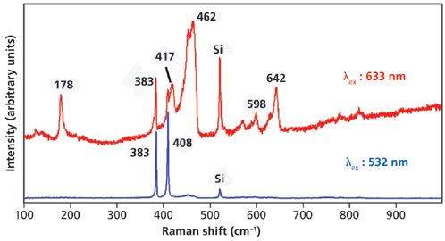
Figure 1: Raman spectra of few-layer MoS2 flake taken at the same location with different excitation wavelengths.
Just as the monolayer and few-layer 2D crystal structure of MoS2 affects the electronic structure, particularly the nature of the bandgap, the vibrational modes are also affected. The first-order Raman bands listed above are for bulk MoS2. However, these bands shift to different energies progressively as the structure changes from approximately six layers down to a single monolayer. The E22g band has been observed to shift progressively from 32 cm-1 in the bulk to 23 cm-1 in the single "trilayer" (16). The term trilayer derives from the fact that MoS2 is not a planar compound; that is, the Mo and S atoms are not all in the same plane. So, a plane of S atoms can be envisioned on the surface with a plane of Mo atoms above that plane and another plane of S atoms above the Mo one; hence the term trilayer. Also, the band positions and respective separations of the E12g and A1g bands show progressive changes from the bulk to a single layer. The E12g (383 cm-1) band shifts to higher wavenumbers and the A1g (408 cm-1) band shifts to lower wavenumbers in progressing from the bulk to a single trilayer corresponding to a band separation of 25 cm-1 to 19 cm-1, respectively (17).
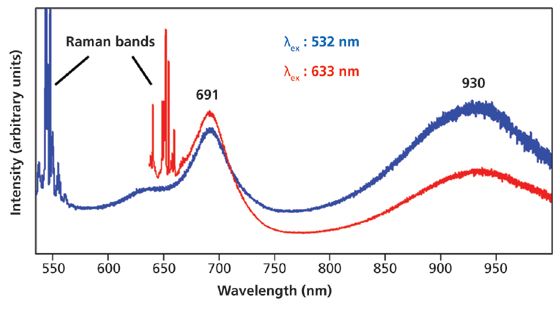
Figure 2: Photoluminescence and Raman spectra of few-layer MoS2 flake taken at the same location with different excitation wavelengths.
The changes of Raman band position with the number of molecular layers described above are most readily observed when using a 532-nm or shorter wavelength excitation. The Raman spectra obtained when using 632.8-nm light to excite few-layer MoS2 appear quite different because of coupling with the aforementioned A1 excitonic transition and the subsequent resonance enhancement. The activity of the harmonic and combination modes yield a richer spectrum and the determination of the number of trilayers present is determined from both changes in band shape and relative intensities (18,19).
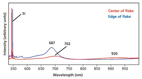
Figure 3: Photoluminescence and Raman spectra of few-layer MoS2 flake taken at different locations on the same flake.
Resonance Raman Scattering and Photoluminescence of Few-Layer MoS2
Exfoliated few-layer flakes of MoS2 are typically heterogeneous, and so the Raman and photoluminescence spectra tend to spatially vary on the flake. Nevertheless, there are spectra that can be considered representative of few-layer MoS2 and they are shown in Figure 1. These spectra were acquired at the same location from the interior of a MoS2 flake, but with different excitation wavelengths. The spectrum acquired with 532-nm excitation is typical of those reported in the literature; it consists primarily of the E12g band at 383 cm-1 and the A1g band at 408 cm-1 as well as the Si substrate Raman band at 520 cm-1. In contrast, the spectrum generated with 632.8-nm excitation is striking insofar as it consists of the same first-order bands and those due to harmonics and combination modes. Remember that the absorption spectrum of MoS2 contains fine structure with narrow absorption peaks at 1.9 eV (653 nm) and 2.1 eV (590 nm) related to d-to-d orbital transitions split by spin-orbit coupling and designated A1 and B1 excitons, respectively (8,15). Consequently, the 632.8-nm excitation couples into the A1 transition producing a resonance enhancement of all of the additional modes observed in Figure 1. All of the bands in the spectrum excited with 632.8-nm light can be accounted for and have previously been assigned (8,12,15).
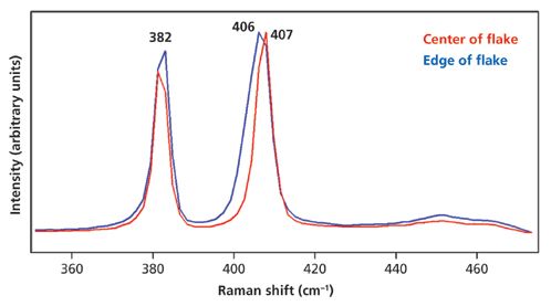
Figure 4: Raman spectra of few-layer MoS2 flake taken at different locations on the same flake. These are the same locations from which the photoluminescence spectra in Figure 3 were obtained.
The effect of excitation wavelength on the photoluminescence spectra of few-layer MoS2 flakes can be seen in the spectra shown in Figure 2. The spectra were acquired at the same location on the flake and are plotted on arbitrary intensity scales to better show the differences in relative strengths of both the photoluminescence and Raman signals. There are several differences to observe that relate to the electronic transitions and their coupling to the few-layer MoS2 flake phonons. The photoluminescence excited at 532 nm is substantially weaker relative to the Raman scattering when compared to the photoluminescence-Raman strength ratio of the 632.8-nm excited spectrum. Furthermore, the relative strengths of the 691- and 930-nm emissions are inverted for the 532- and 632.8-nm excitation wavelengths. An important aspect of this measurement is that one can simultaneously obtain a Raman spectrum and a photoluminescence spectrum from the same location. That fact holds important implications for the ability to simultaneously perform photoluminescence and Raman imaging of few-layer MoS2.
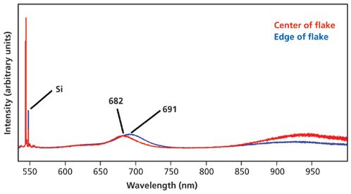
Figure 5: Photoluminescence and Raman spectra of few-layer MoS2 flake taken at different locations on the same flake.
As we noted earlier, the structure of few-layer MoS2 films vary spatially and the most prominent changes appear at the edges. Photoluminescence spectra excited with 532-nm light obtained near the center and edges of a few-layer MoS2 flake are shown in Figure 3. There are substantial differences in the emission spectra, specifically the emergence of an emission maximum at 687 nm and the absence of the 930-nm peak at the edge. Also, note that the Si Raman band from the flake edge is significantly stronger than its counterpart in the flake center spectrum. That difference can be attributed to either fewer layers at the edge, a change in the absorptivity of MoS2 at that location, or both. Note too that the second-order Raman bands that appear between 550 and 575 nm are strong at the flake edge, whereas they are absent in the spectrum from the flake center. These are the bands that appear prominently in the 632.8-nm excited Raman spectrum, so a change in the electronic properties of the flake edge is indicated. That portion of the Raman spectrum consisting of the E12g and A1g bands from these same locations are shown in Figure 4. We can see from the band positions and their separation of 24–25 cm-1 that the thicknesses at these positions are greater than four trilayers (17). However, what is noteworthy is the slight broadening to lower wavenumber of the A1gband at the flake edge such that the peak maximum is now at 406 cm-1. The differences in the Raman and photoluminescence spectra may be an indication of a structural difference at this particular edge location. Furthermore, it appears that there may be a correlation between the Raman scattering and photoluminescence of few-layer MoS2.
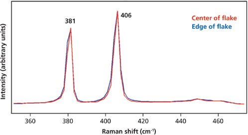
Figure 6: Raman spectra of few-layer MoS2 flake taken at different locations on the same flake. These are the same locations from which the photoluminescence spectra in Figure 5 were obtained.
To investigate this hypothesis, let's look at Figure 5, which shows spectra from center and edge positions taken on another few-layer MoS2 flake. There appears to be little difference between photoluminescence and Raman scattering, particularly the second order modes, as a function of flake position. Furthermore, the corresponding Raman E12g and A1g bands in Figure 6 are identical. Therefore, it seems that a correlation may exist between the Raman scattering and the photoluminescence of few-layer MoS2.
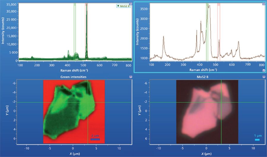
Figure 7: Raman image of few-layer MoS2 flake obtained with 632.8-nm excitation. Red corresponds to the substrate Si and the green intensities correspond to the spatially varying strength of the Raman band at approximately 450 cm-1.
Resonance Raman Imaging of Few-Layer MoS2 Flakes
In the previous section, we compared photoluminescence and Raman spectra of MoS2 taken at the center and edge of few-layer flakes and saw evidence for spatial variation of the solid-state structure. Here, we apply Raman and photoluminescence imaging to compare the spectral and structural differences revealed through spectroscopy to the contrast observed when viewing the flakes with reflected white light microscopy. A collection of hyperspectral data from a few-layer MoS2 flake is shown in Figure 7. A reflected white light image of the flake appears in the lower right hand corner and a Raman image corresponding to the reflected light image appears to its left. The plot on the upper left consists of all of the Raman spectra acquired over the image area and the upper right hand plot is of the single spectrum associated with the cross-hair location in the Raman and reflected light images. The Raman data were acquired using 632.8-nm excitation and a 100× Olympus objective and by moving the stage in 200-nm increments over an area of approximately 13 μm × 13 μm. The Raman image is actually a rendering of signal strength for a particular Raman band as a function of position on the sample. In this particular case, the Raman image is rendered through a color coded plot of Raman signal strength over the corresponding color bracketed Raman shift positions in the two upper traces.
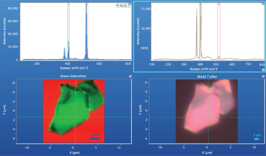
Figure 8: Raman image of few-layer MoS2 flake obtained with 532-nm excitation. Red corresponds to the substrate Si and the green intensities correspond to the spatially varying strength of the Raman band at approximately 408 cm-1.
The red brackets surround the Raman band of Si at 520 cm-1. Consequently, the area surrounding the few-layer MoS2 flake appears red. The green bracket covers the Raman scattering near 450 cm-1, which is assigned to the second order longitudinal acoustic mode at the M point of the Brillouin zone (2LA(M)) of MoS2 (12). This and the other second order modes are prominent in the spectrum because of resonance enhancement. The Raman image in the lower left corner in Figure 7 is presented in a color overlay mode, and the substrate Si signal is attenuated by the MoS2 flake above it. Thus, there is little mixing of red with the green in the Raman image of the flake. The spatially varying shades of green are related to the overall signal strength of the 2LA(M) band under resonance enhancement. Note the rough correspondence of the Raman image of the few-layer MoS2 flake with the spatially varying contrast in the reflected white light image. Of course, the bright green areas correspond to much stronger Raman scattering at that location and the darker areas correspond to a weaker Raman signal. What cannot be seen in a still-frame Raman image is the spatial variation of the band shapes and relative intensities. Interactively changing a bracket selection for width and position in the hyperspectral data set, including selecting ratios of two brackets, allows one to render different resonance Raman images that can reveal spatially varying solid-state structure and electronic properties. The better approach to image the spatial variation of the band structure is through real-time imaging while sliding the color bracket selector over different Raman bands.

Figure 9: Side-by-side comparison of Raman images of the same few-layer MoS2 flake based on different Raman bands and acquired using different excitation wavelengths. Left: 532-nm excitation; Right: 632.8-nm excitation.
The spectra and image shown in Figure 7 were obtained using 632.8-nm (1.96-eV) excitation. That energy occurs right between two excitonic transitions in the absorption spectrum of bulk MoS2, the so-called A1 and B1 excitons at 1.88 eV and 2.06 eV, respectively (8,15,20,21). Thus, 632.8-nm excitation allows one to achieve resonance with the MoS2 A1 excitonic transition and thereby produce resonance Raman enhancement of first and second order vibrational modes of MoS2. Off-resonance Raman scattering can be obtained using 532-nm excitation. A collection of hyperspectral data from a few-layer MoS2 flake obtained with off-resonance 532-nm excitation is shown in Figure 8. The Raman data were acquired using 532-nm excitation and a 100× Olympus objective and by moving the stage in 200 nm increments over an area of approximately 13 μm × 13 μm. The spectra consist primarily of the E12g (383 cm-1) and A1g (408 cm-1) MoS2 bands and the first-order optical phonon from Si at 520 cm-1. Here, red corresponds to the Si substrate and green to the A1g (408 cm-1) MoS2 band. Without resonance Raman enhancement, the spatially varying contrast in the Raman image is found to correspond to the signal strength of the 408 cm-1 band without the changes in relative intensities and band shapes observed when excited with 632.8-nm light. All of the spectra in the image manifest band separations of 24–25 cm-1, and so there is no indication of a single trilayer present in this particular MoS2 flake (17).
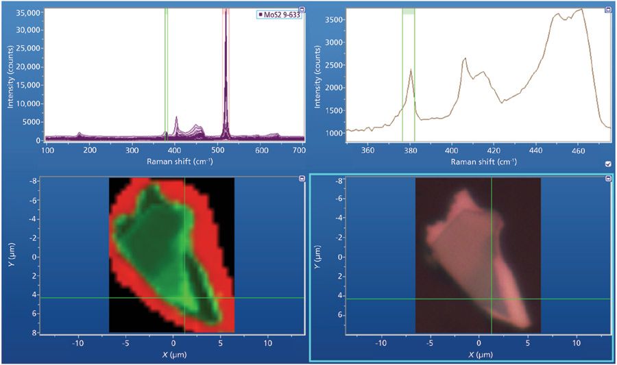
Figure 10: Raman image of few-layer MoS2 flake obtained with 632.8-nm excitation. Red corresponds to the substrate Si and the green intensities correspond to the spatially varying strength of the Raman band at approximately 380 cm-1.
We have imaged the same few-layer MoS2 flake using two excitation wavelengths and rendering the Raman images through the selection of different bands, a first-order mode and a resonantly enhanced second-order mode. The spatially varying intensity of the A1g (408 cm-1) band appears to correspond to varying few-layer MoS2 film thickness when excited at 532 nm. In contrast, the resonance Raman image of the same few-layer MoS2 flake reveals the spatially varying excitonic electronic structure. The Raman images are best viewed side-by-side in Figure 9. From this perspective, we are rendering images to enhance the contrast between off-resonance and resonance Raman scattering corresponding to the film thickness and excitonic electronic structure, respectively.
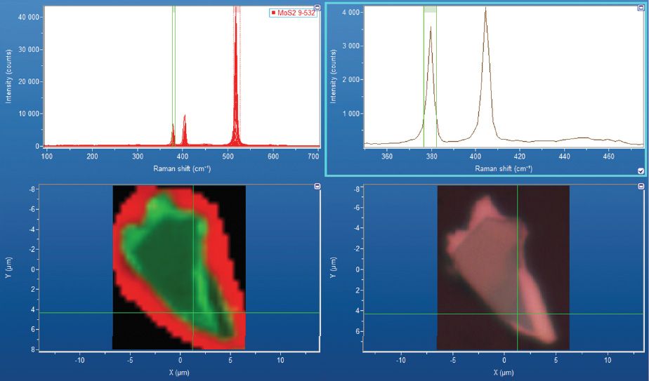
Figure 11: Raman image of few-layer MoS2 flake obtained with 532-nm excitation. Red corresponds to the substrate Si and the green intensities correspond to the spatially varying strength of the Raman band at approximately 380 cm-1.
Of course, another way to render off- and in-resonance Raman images of the few-layer MoS2 flakes is to view them through the bracketing of the same Raman band. A collection of data from a few-layer MoS2 flake is shown in Figure 10. The Raman data were acquired using 632.8-nm excitation and a 100× Olympus objective and by moving the stage in 500-nm increments. The surrounding Si in red is not rectangular because the mapping was performed to follow an irregular shape; this approach allows one to maximize mapping efficiency by analyzing the object of interest without needlessly analyzing the surrounding area. Here the mapping was performed in resonance with 632.8-nm excitation and the E12g (383 cm-1) band was bracketed to render the Raman image in the lower left corner of Figure 10. The single Raman image reveals the spatially varying signal strength of the E12g band; however, it does not reveal the spatially varying complexity of band structure and relative strengths of the first- and second-order modes. A portion of the spectrum corresponding to the cross hairs can be seen in the upper right hand corner. This same MoS2 flake was mapped with 532-nm excitation, and the entire hyperspectral data set is shown in Figure 11. Here, we render a Raman image by bracketing the same E12g and Si bands as in Figure 10. So now we have a direct comparison of the resonance and off-resonance Raman images of a few-layer MoS2 flake based on the same first-order Raman band. The cross hair has been placed in the exact same position of Figures 10 and 11 for a comparison of the resonance and off-resonance Raman spectra from the same location in the flake. The spectral differences are quite striking. Even when bracketing the same Raman bands, the resonance and off-resonance Raman images that are rendered are sufficiently different to reveal the spatial heterogeneity of the few-layer MoS2 flake.
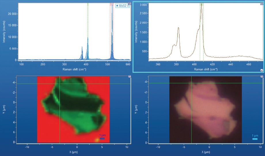
Figure 12: Raman image of few-layer MoS2 flake obtained with 532-nm excitation. Red corresponds to the substrate Si and the green intensities correspond to the spatially varying strength of the Raman band at approximately 408 cm-1. Note the strain components in the upper-right-hand corner spectrum.
Strain Imaging
Thus far, the 532-nm excited spectra that we examined have consisted of bands that are fairly sharp and symmetric. However, with sufficiently high spectral resolution one can observe band broadening and asymmetry, thereby indicating strain, at certain locations within a few-layer MoS2 flake and even throughout an entire flake. A Raman image obtained with 532-nm excitation is shown in Figure 12. The Raman data were acquired using a 100× Olympus objective and by moving the stage in 300-nm increments over an area of approximately 13 μm × 13 μm. The red brackets surround the Raman band of Si at 520 cm-1. Consequently, the area surrounding the few-layer MoS2 flake appears red. The green bracket covers the Raman scattering of the A1g (408 cm-1) band. The A1g rendered Raman image comports well with the contrast observed in the reflected white light image. There is a direct correlation of the shapes and locations of the contrasting regions in the reflected white light image with the Raman image. Nevertheless, the reflected light bright and dark regions do not necessarily correlate directly to strong Raman scattering at the same location on the flake. Sometimes, a dark area in the reflected white light image corresponds to strong Raman scattering as in the diagonal streak in the northwest corner of the flake. In addition, note the spectrum in the upper-right-hand corner associated with the cross hair location in the images. You see a strain component to the low energy side of both the E12g (383 cm-1) and A1g (408 cm-1) bands. Strain that can be clearly seen in the spectra from a Raman image does not reveal itself in the reflected white light image.
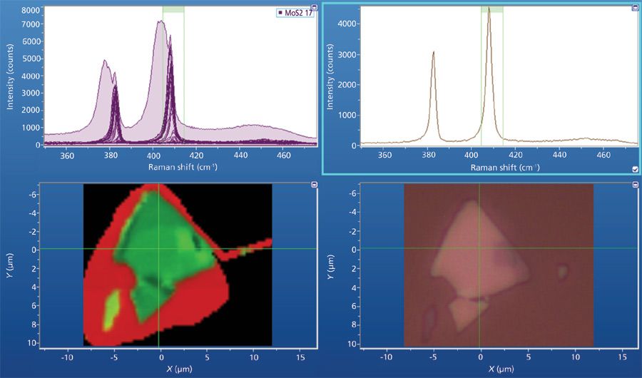
Figure 13: Raman image of few-layer MoS2 flake obtained with 532-nm excitation. Red corresponds to the substrate Si and the green intensities correspond to the spatially varying strength of the Raman band at approximately 408 cm-1.
In some few-layer MoS2 flakes, strain can be observed in the Raman spectra along edges and even throughout the entire flake. A good example of this is shown in Figure 13. The Raman data were acquired using 532-nm excitation and a 100× Olympus objective and by moving the stage in 300-nm increments. The Raman spectrum at the cross hairs, near the center of the flake, consists of sharp symmetric bands. However, there is a substantial number of bands in the hyperspectral data set (upper-left-hand frame) that are broadened and shifted. Those "strain" spectra were found almost entirely at the upper-left edge of the large flake and throughout the small yellow flake in the Raman image. Raman spectra obtained from the center and edge of the large flake and the center of the small flake in the lower-left corner are shown in Figure 14. Note that both the E12g and A1g bands shift and broaden in the same direction to a lower wavenumber. Therefore, we can properly conclude that these spectral changes indicate strain rather than a reduction in the number of MoS2 layers.
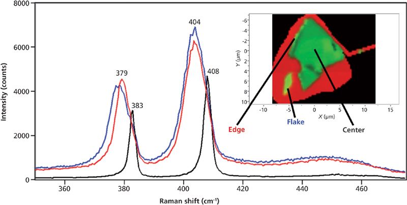
Figure 14: Raman spectra of few-layer MoS2 from different locations on the flake shown in Figure 13. Note the substantial shifts and broadening corresponding to strain.
Structure at the Perimeter
The large MoS2 few-layer flake in Figure 13 exhibited strain along a portion of the perimeter. An interesting fact is that very often the structure of the perimeter of few-layer MoS2 flakes is quite different from that of the interior, manifesting differences in both Raman scattering and photoluminescence. A collection of data from a few-layer MoS2 flake is shown in Figure 15. The Raman data were acquired using 532-nm excitation and a 100× Olympus objective and by moving the stage in 300-nm increments. A reflected white light image of the flake appears in the lower-right-hand corner and a Raman image corresponding to the reflected light image appears to its left. Here we have used the green brackets to highlight the strain free A1g band and the blue brackets to cover the lower wavenumber broadened side of the A1g band to reveal locations of strain in the flake. Note that the entire perimeter of the flake appears blue in the Raman image because of the presence of strain. It is noteworthy that strain that can be clearly seen in the spectra from a Raman image does not reveal itself in the reflected white light image.
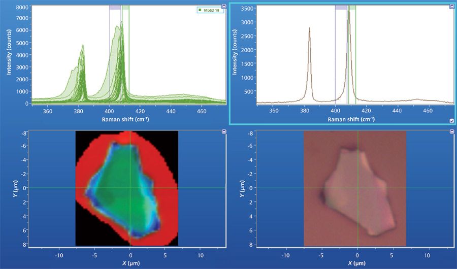
Figure 15: Raman image of few-layer MoS2 flake obtained with 532-nm excitation. Red corresponds to the substrate Si and the green intensities correspond to the spatially varying strength of the Raman band at centered at 408 cm-1. The blue bracket to the low energy side of the 408 cm-1 band reveals the strain component clearly seen at the perimeter of the flake in the Raman image.
We find that the use of 532-nm excitation is most useful for identifying strain through the broadening and shifting of the E12g and A1g bands. However, the use of 632.8-nm excitation in resonance with the MoS2 A1 excitonic transition also reveals structural differences at the perimeter. A collection of data from a few-layer MoS2 flake is shown in Figure 16. The Raman data were acquired using 632.8-nm excitation and a 100× Olympus objective and by moving the stage in 200-nm increments over an area of approximately 8 μm × 8 μm. A reflected white light image of the flake appears in the lower-right-hand corner and a Raman image corresponding to the reflected light image appears to its left. The plot on the upper left consists of all of the Raman spectra, including a photoluminescence component, acquired over the image area. The upper-right-hand plot is of the single spectrum associated with the crosshairs location in the region showing photoluminescence. The Raman image is rendered using the green color brackets to capture the A1g band and the blue brackets surround the broad photoluminescence. Even in the resonance Raman image, the A1g band manifests a greater intensity at the perimeter than it does in the flake interior. Also, we see a light blue region in the upper-right corner of the flake corresponding to the emission centered at 678 nm (1050 cm-1 Raman shift). This region appears light blue in the spectral image because there are contributions from A1g Raman scattering (green) and the 678-nm photoluminescence (blue) from the same locations. So, with the selection of the appropriate excitation wavelength, one can simultaneously perform resonance Raman and photoluminescence spectral imaging of few-layer MoS2.
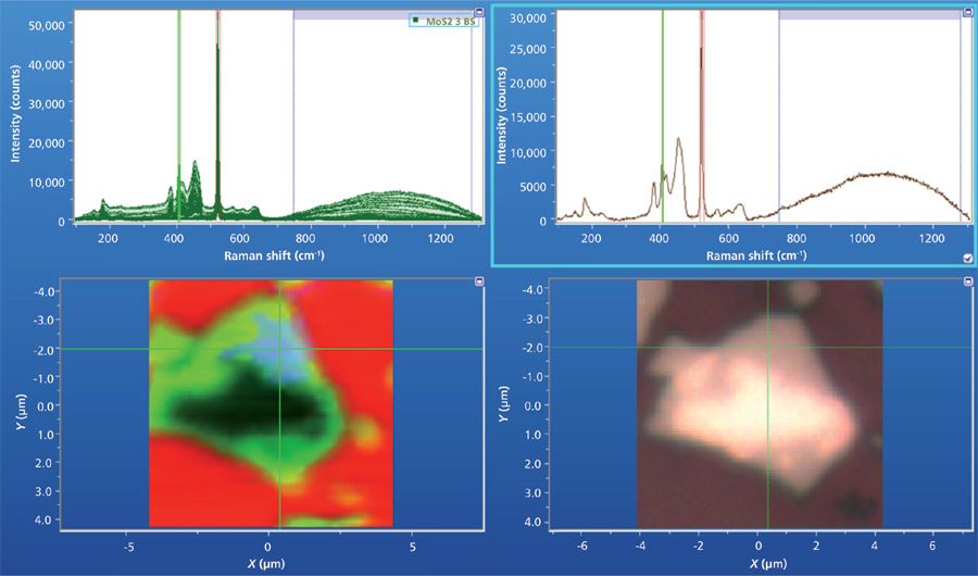
Figure 16: Raman image of few-layer MoS2 flake obtained with 632.8-nm excitation. Red corresponds to the substrate Si and the green intensities correspond to the spatially varying strength of the Raman band at centered at 408 cm-1. The blue bracket captures the photoluminescence, which can be seen primarily in the northeastern quadrant of the flake in the Raman and photoluminescence image.
Conclusions
We compared photoluminescence and Raman spectra of MoS2 taken at the center and edge of few-layer flakes and saw evidence for spatial variation of the solid-state and electronic structure. We applied Raman, resonance Raman, and photoluminescence hyperspectral imaging to observe spatially varying structural differences that are not revealed through reflected white light microscopy. The selection of the appropriate excitation wavelength allows one to simultaneously perform resonance Raman and photoluminescence spectral imaging of few-layer MoS2. That ability should allow materials scientists to better design and fabricate electronic and optoelectronic devices based on few-layer MoS2.
References
(1) D. Jariwala, V.K. Sangwan, L.J. Lauhon, T.J. Marks, and M.C. Hersam, ACS Nano8, 1102–1120 (2014).
(2) G. Eda and S.A. Maier, ACS Nano7, 5660–5665 (2013).
(3) R. Ganatra and Q. Zhang, ACS Nano8, 4074–4099 (2014).
(4) H. Li, J. Wu, Z. Yin, and H. Zhang, Acc. Chem. Res.47, 1067–1075 (2014).
(5) H. Li, J. Wu, X. Huang, G. Lu, J. Yang, X. Lu, Q. Xiong, and H. Zhang, ACS Nano7, 10344–10353 (2013).
(6) K.F. Mak, C. Lee, J. Hone, J. Shan, and T.F. Heinz, Phys. Rev. Lett. 105, 136805 (2010).
(7) A. Splendiani, L. Sun, Y. Zhang, T. Li, J. Kim, C.-Y. Chim, G. Galli, and F. Wang, Nano Lett.10, 1271–1275 (2010).
(8) A.M. Stacy and D.T. Hodul, J. Phys. Chem. Solids46, 405–409 (1985).
(9) J.R. Ferraro, Appl. Spec.29, 418–421 (1975).
(10) S. Jimenez Sandoval, D. Yang, R.F. Frindt, and J.C. Irwin, Phys. Rev.B44, 3955–3962 (1991).
(11) T.J. Wieting and J.L. Verble, Phys. Rev. B3, 4286–4292 (1971).
(12) J.M. Chen and C.S. Wang, Solid State Commun.14, 857–860 (1974).
(13) S. Sugai and T. Ueda, Phys. Rev. B26, 6554–6558 (1982).
(14) D.O. Dumcenco, K.Y. Chen, Y.P. Wang, Y.S. Huang, and K.K. Tiong, J. Alloys Compounds506, 940–943 (2010).
(15) B.C. Windom, W.G. Sawyer, and D.W. Hahn, Tribol. Lett.42, 301–310 (2011).
(16) Y. Zhao, X. Luo, H. Li, J. Zhang, P.T. Araujo, C.K. Gan, J. Wu, H. Zhang, S.Y. Quek, M.S. Dresselhaus, and Q. Xiong, Nano Lett.13, 1007–1015 (2013).
(17) C. Lee, H. Yan L.E. Brus, T.F. Heinz, J. Hone and S. Ryu, ACS Nano 4 2695-2700 (2010).
(18) K. Golasa, M. Grzeszczyk, R. Bozek, P. Leszczynski, A. Wysmolek, M. Potemski, and A. Babinski, Solid State Commun.197, 53–56 (2014).
(19) B. Chakrabory, H.S.S. Ramakrishna Matte, A.K. Sood, and C.N.R. Rao, J. Raman Spectrosc.44, 92–96 (2013).
(20) R. Coehoorn, C. Haas, and R.A. de Groot, Phys. Rev. B35, 6203–6206 (1987).
(21) G.L. Frey, R. Tenne, M.J. Matthews, M.S. Dresselhaus, and G. Dresselhaus, Phys. Rev. B 60, 2883–2892 (1999).
David Tuschel is a Raman applications manager at Horiba Scientific, in Edison, New Jersey, where he works with Fran Adar. David is sharing authorship of this column with Fran. He can be reached at: david.tuschel@horiba.com

David Tuschel

AI-Powered SERS Spectroscopy Breakthrough Boosts Safety of Medicinal Food Products
April 16th 2025A new deep learning-enhanced spectroscopic platform—SERSome—developed by researchers in China and Finland, identifies medicinal and edible homologs (MEHs) with 98% accuracy. This innovation could revolutionize safety and quality control in the growing MEH market.
New Raman Spectroscopy Method Enhances Real-Time Monitoring Across Fermentation Processes
April 15th 2025Researchers at Delft University of Technology have developed a novel method using single compound spectra to enhance the transferability and accuracy of Raman spectroscopy models for real-time fermentation monitoring.
Nanometer-Scale Studies Using Tip Enhanced Raman Spectroscopy
February 8th 2013Volker Deckert, the winner of the 2013 Charles Mann Award, is advancing the use of tip enhanced Raman spectroscopy (TERS) to push the lateral resolution of vibrational spectroscopy well below the Abbe limit, to achieve single-molecule sensitivity. Because the tip can be moved with sub-nanometer precision, structural information with unmatched spatial resolution can be achieved without the need of specific labels.