Three-Dimensional Printing and the Art of Making Small Working Prototype Spectrometers
In the past, moving from a concept for an analytical instrument to actually producing a functioning instrument was a relatively tedious and lengthy process. The traditional approach was to draft a design and then go through a number of iterations, along with design reviews and sign-offs. Today, if one has a good designer who is well-versed in computer-aided design (CAD) engineering software, then it is possible to significantly reduce the time to develop a good-looking functional design. However, the time to go from the CAD design to a complete piece of hardware is typically the longest part of the process. It is not unusual for machine shop delays to be up to 6–8 weeks. Today, such delays can be eliminated by producing the designed parts on a desktop with a three-dimensional (3D) printer. This article shows, by example, how a 3D printer can speed up the process of making prototype hardware for a spectral measurement system, shortening the time to produce functional hardware from weeks to days—or less.
The traditional approach to the prototyping of the optics for a spectrometric measurement system is to build the prototype, starting with an optical bench and using off-the-shelf components, such as lenses or mirrors with associated mounts, slit assemblies, source and detector modules, and so on. This approach works for testing out the optical train and allows the optics to be optimized in terms of location, beam direction, and geometry. The next step of the transition to a facsimile of the intended instrument is a little more challenging because although optical components can be obtained from optics houses, such as ThorLabs, Newport, or Edmund Optics, the basic frame and shape of the instrument has to be built up from machined parts. Obtaining the right engineering resource, such as a machinist with experience of building instruments, is not so easy, and it is a skill that is disappearing. However, there is a good practical solution available today that can fill in the gaps and enable a good-looking prototype instrument to be produced, and that is three-dimensional (3D) printing. A 3D printer not only can generate good-looking and well-finished parts, but it can simplify assembly and speed up the prototyping process. This work is made possible by the use of a desktop 3D printer, where the transition from a computer-aided design (CAD) file to a finished part is as simple as a mouse button press, thus eliminating the need to wait for parts to be made at a machine shop. This article illustrates, by practical examples, the advantages gained from 3D printing of prototype parts.
Practical Examples of the Role of 3D Printing for Instrument Prototypes
The following are actual examples of the implementation of 3D printing as used to evaluate prototype spectral measurement concepts. As an important note, these examples are now more than 10 years old, and in terms of the technology of 3D printing, they are by no means state of the art. The technology of 3D printers and printing substrates has advanced by leaps and bounds in recent years. However, the concept and rationale for its use remains the same.
Example 1
The first assembly, shown in Figure 1, involved in situ measurements on a custom extraction device with a hydrophobic membrane supported on a metal mesh. The membrane was used as the extraction medium for the isolation and direct measurement of organic contaminants in water. An issue for the measurement was the need to measure everything in situ in the presence of a high degree of optical scattering from the supported membrane. The goal was to make the measurement without the need for any additional focusing optics.
FIGURE 1: (a,b) Measurement system for organic contaminants extracted from water, showing the various design elements listed and (c) the detector.
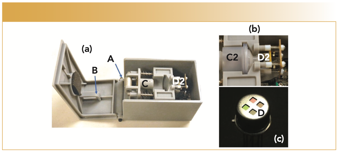
Here, the most important considerations were to rigidly retain and locate the membrane sampler, shown as C2 in Figure 1, to bring the infrared (IR) source (C) into close (and reproducible) proximity to the supported membrane, and to locate the exit of the IR radiation (D2) immediately in front of the quad detector (D). This design helps to concentrate the highly attenuated IR beam, passing though the membrane on to the four-channel detector (shown as D2 and D) without any supplemental focusing optics. The detector assembly provides four electronically independent channels representing the unique analytical wavelengths as defined by narrow bandpass filters mounted in front of the detector elements.
This design was simple and effectively inexpensive for a four-channel non-dispersive IR (NDIR) instrument. Figure 1a shows the system open with all relevant components shown and the membrane sampler location unoccupied, ready to receive a sample for analysis. Once the sampler is loaded, the lid and an actuation cam (B) is closed around hinge (A). In Figure 1b, the cam pushes the IR source assembly into the sampler (C2), making it ready to be measured by the quad detector (D2). The ability to reproduce the exact mode of measurement was invaluable, and it simplified the final instrument design, saving both time and prototyping costs. Figure 1c is a close-up of the four-channel detector.
Example 2
The concept being prototyped here in Figure 2 is equivalent to the electronic nose system of measurement where gases and vapors are detected by the unique responses of individual channels made up of electrically conductive polymer membranes. In such systems, there are at least eight or nine (possibly more) individual channels that each give a unique set of responses for the compounds detected in the ambient air being sampled. In the example being prototyped here, the conductive polymer membranes are replaced by IR detectors that are responsive to specific wavelengths. Like in example 1, the wavelengths are defined for each quad detector by a set of narrow bandpass IR filters. Unlike the previous example, this system features four quad detectors, providing a total of 16 unique detection channels. The wavelengths selected cover a nominal spectral range from 2.5 μm (2500 nm or 4000 cm-1) to 16.67 μm (16,670 nm or 600 cm-1). Three of the wavelengths represented common IR absorptions for C-H, carbon monoxide (CO) and carbon dioxide (CO2). The rest of the wavelengths selected were spread over the full range and included the statistically most relevant absorptions. Conceptually, this prototype can may be considered to be an improvement over the conductive polymer system because a correlation to known spectral absorption wavelengths can be established. One relevant thought here is that we are dealing with molecular vibration-based IR absorptions, and the olfactory system (smells and odors) responses are also linked to molecular vibrations.
FIGURE 2: An electronic nose simulation with a 16-channel ambient air monitor: (a) PCB layout, (b) integrated nose sensor unit, and (c) output results.
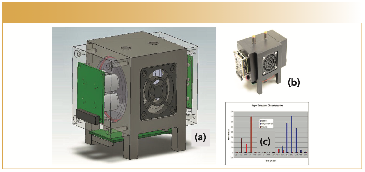
The assembly developed (Figures 2a and 2b) is designed to be a standalone ambient air monitoring system, with 16 independent channels, as described above. The key components of the system are exposed in the “semi-transparent” version designated (Figure 2a). The spectral measurements are obtained from four quad detectors (four channels each). In this particular case, each quad is equipped with its own IR source, with the electronics set up to monitor the output of the detectors providing a set of 16 signals, representing 16 different sets of wavelengths. The system monitors the air, which is drawn in by a fan assembly on the side of the measurement chamber. Then, 16 sets of absorbance data are generated and these are normalized and presented in a histogram form (Figure 2c). In this particular example, the 3D printing provides the frame of the overall assembly and the measurement chamber that is coupled to the fan used to transport the air into the chamber. The IR beams from the individual sources transverse the chamber, with a 50-mm optical path, which is sealed at both ends with IR-transmitting windows.
Again, in this case, the 3D printing provided a testing platform that enabled the overall measurement concept to be evaluated.
Example 3
Ambient air monitoring is intended to measure and monitor low concentrations of gases and vapors in the air. For the nose simulation, a relatively short optical path was used for the measurement. Although this process was effectively multiplexed with the simultaneous measurement of 16 channels the sensitivity for individual species may have been limited by the optical measurement path. For the IR measurement of individual gases (vapors) at low concentrations, it is beneficial to extend optical path to a meter or more. When working with a small measurement system, a 1-m path (or greater) can be difficult to implement within a limited space. The popular “White Cell” has been used for such measurements; however, it can yield a relatively large measurement volume. The system shown in Figure 3 was devised to enable long path measurements, of one to two meters, while maintaining a small internal measurement volume. When optimized, the cell has 4x to 5x less volume than the comparable pathlength “White Cell.”
FIGURE 3: (a,b) Compact 1-m multipass gas cell showing various design elements listed, and (c) a 1-m standalone monitor.
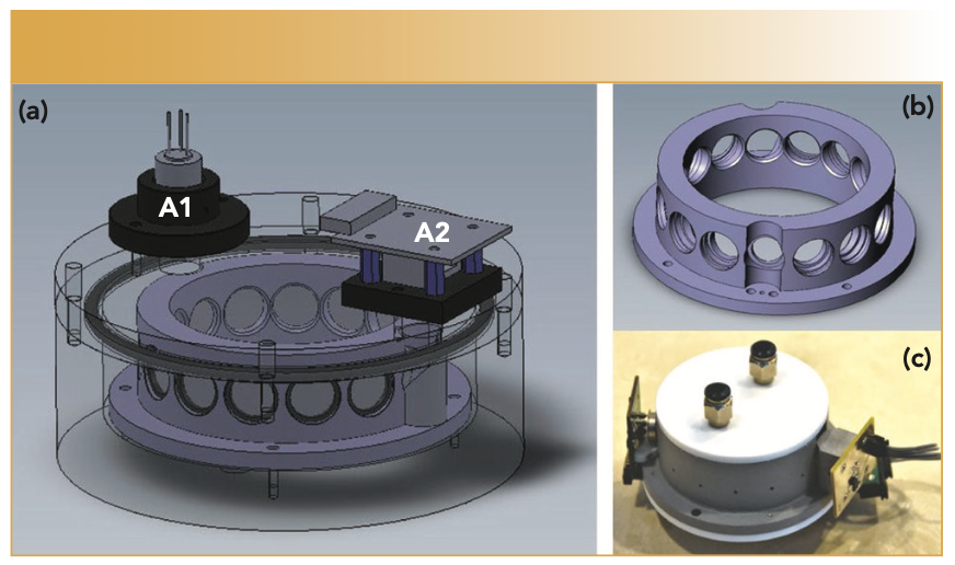
The system shown in Figure 3a (A1/A2) is a packaged design for continuous monitoring applications where the main measurement component, a ring containing 13 mirrors (Figure 3b), is housed within a cylindrical enclosure chamber. In this case, the IR beam is injected into the chamber with an IR source mounted at A1, and is collected at A2 following multiple passages, with reflections from the mirrors mounted in the walls of the ring (Figure 3b). The beam is directed in and out of the enclosure with a pair of off-axis paraboloid mirrors (one in and one out). The ring in this case is 3D printed with the mirror recesses designed to provide an exact push fit for the mirrors. The dimensions are exact to provide a 1-m path following the multiple reflections. This design is unique insofar as it provides for a quick and easy assembly with all 13 mirrors pre-aligned with no additional alignment required.
A modified version of the ring mount is shown in Figure 3c. In this version, the ring also forms the external part of the enclosure, where the IR beam enters and exits on the horizontal axis. For this variant, the beam enters directly from the source and exits at a quad detector, both equipped with their own electronic interfaces. With the exception of these electronic components, the rest of the enclosure components are 3D printed, which are shown in gray and white. Note that the gray component is actually printed from a 50:50 polyamide:aluminum blend. The blend was preferred in this case because the aluminum helped improve the thermal characteristics of the overall package. The benefit provided in this case by the 3D printed part was that it simplified assembly, and it eliminated the need for optical alignment (by design).
Example 4
In 2015, I gave a webinar on new technical advances in optical spectroscopy. At the end, a participant asked if a technology could be recommended for a Hadamard Transform spectrometer. The answer back was that a technology, such as the Texas Instruments (TI) digital light processing (DLP) chip, could be a potential solution to encoding spectral data for a Hadamard transform. It turned out that not only could the DLP enable Hadamard encoding, but it could also be applied to the design of a spectrometer and eliminate the need for a detector array. This was an unanticipated benefit because it enabled a spectrometer to be developed in a wavelength range that required an expensive array, and it enabled a higher pixel count than such high-cost arrays. A good example is the elimination of the costly extended InGaAs array from a long wavelength NIR spectrometer. In this case, a high-performance single element detector would be used in place of the array. In this case, the DLP provides the array function by collecting the dispersed NIR radiation from a planar grating, and with wavelength selection being made by addressing the individual or groups of programmable reflective pixels.
This resulted in the development of an NIR spectrometer platform based on TI’s DLP technology. It should be pointed out that not all spectral ranges benefit from the use of the DLP scanning. For example, the standard charged-coupled device (CCD) array UV-vis-NIR systems use relatively low cost, high resolution arrays and, in such cases, there is no gain from the use of a DLP. However, the benefits of DLP scanning for the long-wave NIR enables a spectrometer to be designed that covers the spectral range of 1300–2600 nm. An added benefit gained for this spectral range is that extended InGaAs requires cooling to obtain the best noise performance. Changing from an array to a single element detector significantly reduces the thermal overhead, as well as cost of implementation.
It is important to note that TI does not make instruments; it produces advanced computer chips. For the DLP technology to be evaluated, TI designed a functional optical bench and this design was made available to instrument developers and researchers. The evaluation system that was made available is shown in Figure 4. This system had a conventional design, which turned out to be difficult to assemble because each optical component required adjustment and alignment; these alignment components can be seen in Figure 4a.
FIGURE 4: (a,b) Conventional design and the (c) 3D printed optical bench design.
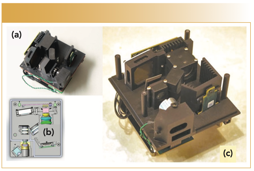
In a collaboration with TI, a new lens recipe was generated based on the use of seven spherical lenses (instead of six aspherical lenses), and this resulted in a significant cost reduction. The optical layout with the spherical optics is shown in Figure 4b. It was realized that an alternative approach to the assembly could be adopted if the optical bench could be fabricated as a single component without the individual optical subassemblies. Yes, this was made possible by a transition to a 3D printed part for the optical base. A 3D printed version of an assembled instrument is shown in Figure 4c, and the components that required alignment by the conventional approach (Figure 4a) can be seen on this assembly, but no alignment is required. All lenses are just inserted into slots and are pre-aligned and optimized.
Was this transition a success? The answer was yes and no. It was possible to make one-off prototypes that performed well. However, at the time, it was hoped that a product could be made directly with this simplified 3D printed baseplate. The main issues came down to limitations of the 3D printing materials in terms of making threaded parts and thermal conductivity. These issues limited the reproducibility of optical alignments, particularly for the grating. The timeframe for this work was late in 2018. We are four years further on now with significant improvements in 3D printers and 3D printing materials. With an optimistic view, it is anticipated that many of the original goals here for instrument manufacturing can be met.
Summary and Conclusion
The application of 3D printing has been described in context of a prototyping and concept-proving tool. The examples shown have been limited by both “age” of hardware and materials, and the ability to describe the end-application in depth because of commercial proprietary issues. Although the examples described may appear to lack style, they were all functional and proved a point. Important early limitations were the need to use special fastening aids to enable fixtures, such as screws to be used, the inability to make metal parts and the lack of materials to make optical components, such as lenses. The closest thing to metal parts were made from a 50:50 blend of polyamide and aluminum. Most of the other structural parts were made from selective laser sintering (SLA) grade polyamide.
Today, it is possible to purchase a desktop 3D printer for a couple of thousand dollars, and so conceptually concepts and applications can be tested in “real-time”. In other words, no need to wait for parts to come back from a machine shop or an external contractor. The implied ability to transition from conceived idea to functional prototypes and on to manufactured products can be realized today. Also, the material and fabrication limitations cited above, for the most part, have been addressed. For example, both metal parts and transparent small optical parts can be produced from commercial 3D printers. Examples of 3D printed micro-spectrometers operating in the visible spectrum have been published. However, as an important caveat, it is possible that spectral measurements that require optical transparency in certain wavelength regions may not be available, at least for now, who knows what might exist in a year or two.
Final Thoughts
It has been a while since I have written an article for Spectroscopy. I have shared a long-term working relationship with the magazine, going back several decades. During that time, the nature and volume of my work in spectroscopy, and the science itself, have changed significantly. Normally, I write and document in the third person, but for this article, I have deviated from this and written in both the first and third person.
My background and training were in analytical chemistry, and over time became focused on spectroscopy. However, in the 1980s I started the transition to instrumentation, with some focus on optics, opto-mechanics, and spectral data handling. Coates Consulting was established in the mid-1990s, leading to a specialization on measurement technologies and small, low-cost instrumentation.
A few months back, the editorial staff contacted me to see if I could put together an article or two on technologies tied to spectral measurements, and in particular, on key technologies that are involved with new instrumentation, such as with the miniaturization or scaling down of spectrometers, and the changes in measurement platforms. The latter involves the move away from the laboratory and toward handheld or distributed measurements involving spectrometers designed as sensors. Having agreed to write the article, I was faced with the challenge of what material I could discuss and what concepts could be presented; in recent years, most of my instrumentation projects have been covered by non-disclosure agreements (NDAs) and confidentiality documents limiting what can be discussed in public.
I started writing this publication at the beginning of July. Over that first weekend, my attention was drawn to an article published in the New York Times entitled “3D Printing Grows Beyond its Novelty Roots,” by Steve Lohr. The case being made was that the technique of 3D printing had jumped from being a tool to make one-off and prototype parts to a full-blown means of making specialized manufactured mechanical parts, with a high degree of “accuracy” and reproducibility. In my opinion, 3D printing has been a game changer for evaluating spectral measurement concepts, and I have reflected on this aspect in this text.
My personal involvement with 3D printing started around 2012. At the time, it was used for making small numbers of prototypes for projects that involved unique or complex designs for spectral measurements. At issue was how to test out a concept without great expense and without risking going down blind alleys if the “guesses” were wrong. All the systems involved making IR measurements, in the near infrared (NIR) and mid-IR spectral regions. For some applications, it is possible to simulate the application on a laboratory instrument. Although that may work for some applications, the approach may not duplicate the exact sampling or data acquisition conditions and may give a false impression relative to the “success” of the application. This situation is where the benefits of 3D printing emerged. A complete measurement system could be designed (with a standard CAD package), assembled and tested, where the 3D printing included the enclosures and assembly structures as well as some of the optical components. For reference, the CAD package used for the projects outlined here was SolidWorks (published by Dassault Systemes).
Disclaimer
The author is not writing this article as an expert in 3D printing; in fact, quite the opposite is true. The article is written from the perspective of a person experienced in the design and implementation of spectroscopic instrumentation and spectral sensing technologies. There is no doubt that many readers may well be more expert in 3D printers and the associated technologies, and so please do not write and complain! I have included several references useful for further information on this subject (1–6).
References and Further Reading
(1) Think 3D Team, 3D Printing Tutorial (PDF): Beginner’s Guide to 3D Printing, version 0.1. https://www.think3d.in/landing-pages/beginners-guide-to-3d-printing.pdf (Accessed 5 December 2022)
(2) Workman Jr., J.; Coates, J.; Naranjo, D. Micromirror spectrophotometer assembly. U.S. Patent 10,054,483, issued August 21, 2018.
(3) Workman Jr., J.; Coates, J.; Naranjo, D. Micromirror spectrophotometer assembly. U.S. Patent 10,309,829, issued June 4, 2019.
(4) Baumgartner, B.; Freitag, S.; Lendl, B. 3D Printing for Low-Cost and Versatile Attenuated Total Reflection Infrared Spectroscopy, Anal. Chem. 2020, 92(7), 4736–4741. DOI: 10.1021/acs.analchem.9b04043
(5) Nesterenko, P.N. 3D Printing in Analytical Chemistry: Current State and Future. Pure and Applied Chemistry, 2020, 92(8), 1341–1355. DOI: 10.1515/pac-2020-0206
(6) Wang L.; Pumera. M. Recent Advances of 3D Printing in Analytical Chemistry: Focus on Microfluidic, Separation, and Extraction Devices. Trends Analyt. Chem. 2021, 135, 116151. DOI: 10.1016/j.trac.2020.116151
John Coates is the principal at John Coates Consulting LLC, in Yarmouth Port, MA. Direct correspondence to: jpcoates@coates-consulting.com ●

LIBS System Built on Microjoule High PRF Laser Identifies Aluminum Alloys for Recycling Potential
January 2nd 2024Differing grades of aluminum alloys have large differences in their composition, especially when it comes to trace elements, emphasizing the need for them to be evaluated for means of production, use, and recycling.