Application of Raman Polarization Selection Rules: Heterogeneous Solid State Structure
Special Issues
The orientation of a crystal can be determined from the phase shift of the experimental P/O micro-Raman diagram relative to that calculated for a particular crystal face.
Micro-Raman spectroscopy is often performed to spatially distinguish materials of different chemical composition in solid samples. However, there are many instances in which the spatial heterogeneity consists not of chemical composition, but of solid-state atomic structure within a material of otherwise uniform composition. Diamond films prepared by chemical vapor deposition (CVD) on silicon wafers present just such a case in which strain, crystallinity, and defects vary spatially. An object can appear to be spectrally uniform if one is not aware of how the degree of crystallinity, strain, or state (amorphous or crystalline) of the matter manifests itself spectroscopically. To access the full benefits of micro-Raman spectroscopy, we show how the spatial heterogeneity of solid-state structure and the orientation dependence of strain in a nominal single crystal of CVD diamond can be characterized through the application of Raman polarization selection rules.
The fabrication of diamond films by chemical vapor deposition (CVD) has been under development for many years now for applications including hardened surfaces, optical windows, and electrodes. The solid-state structure of these films has a direct impact on the material properties and, therefore, figures of merit of the final product. Crystallinity, single or poly, the number of defects, strain, and even the crystal face can affect performance. Furthermore, the uniformity of such films can affect the overall utility of the final product. Therefore, analytical methods are needed that can characterize the spatially varying structure of CVD diamond films.
To that end, we used the application of Raman polarization selection rules for the purpose of simply differentiating single from polycrystalline diamond and to probe the extent of lattice defects, and thereby the degree of disorder, present in a crystal.

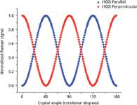
Figure 1: Calculated results for a P/O micro-Raman backscattering experiment for a diamond (100) face.
Results and Discussion
The first figure displays the theoretical results for polarization/orientation (P/O) Raman backscattering from a diamond crystal with the laser beam incident on the (100) face (1). The Raman signal is calculated for configurations with the polarization analyzer parallel and perpendicular as the crystal is rotated in the plane. The experimentally obtained P/O micro-Raman diagram generated by plotting the peak area of the 1333-cm-1 Raman band from a Drukker diamond (serving as our reference) is shown in Figure 2.

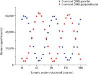
Figure 2: Experimental results for the P/O micro-Raman backscattering experiment with a Drukker diamond (100) face.
The diamond (100) experimental P/O plot consists of two sinusoidal functions 45° out of phase and the plot form is in excellent agreement with the calculated diagram of Figure 1. However, note that calculations predict a maximum response at 0° for the perpendicular configuration, whereas the parallel configuration is near maximum at 0° for the experimentally obtained data. This can be understood in terms of the crystal orientation of the calculation compared to the sample angle with respect to a laboratory reference frame. The approximate 50° phase shift between the experimentally obtained and calculated diamond (100) P/O plots is understood as a difference in the crystallographic starting orientations for data collection. This illustrates an application of P/O micro-Raman spectroscopy for the analysis of texture in natural materials or fabricated devices. P/O plot phase shifts can be used to quantitate the degree of crystallographic orientation or alignment of different features on a micrometer scale relative to a sample orientation and coordinate system in the laboratory reference frame.

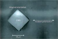
Figure 3: Reflected light image of CVD diamond from which P/O micro-Raman spectra were obtained.
The CVD films consisted of diamond clusters whose edge lengths ranged from ~5 µm to 15 µm. The faces of the diamonds are square and triangular and presumably correspond to the (100) and (111) faces, respectively. We performed P/O micro-Raman spectroscopy on the isolated square faces to demonstrate the utility of this technique for the characterization of CVD diamond crystallinity. A reflected light image of one such square face from which P/O micro-Raman spectra were obtained is shown in Figure 3.

Figure 4: P/O micro-Raman spectra of a (100) face of CVD diamond the light collection analyzer parallel and perpendicular to the incident polarization.
We obtained P/O micro-Raman spectra of diamond films prepared by chemical vapor deposition using a 1.6-mW, 488.0-nm laser beam focused to a 0.6-µm diameter with an Olympus MS Plan 100 (0.95 NA) objective. Raman scattered light was collected using the same microscope objective (backscattering configuration). An analyzer was placed in front of the spectrometer entrance slit and configured either parallel or perpendicular to the incident polarization. Individual spectra were collected at 5° rotational increments for each analyzer polarization configuration as the sample was rotated within the focal plane. The sensitivities of the microscope and spectrometer to the two, orthogonal polarizations were characterized against a depolarized white light source. Accordingly, corrections were made to the intensities of P/O micro-Raman spectra obtained at the corresponding polarizations.

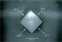
Figure 5: Reflected light image of CVD diamond showing the assignment of crystallographic faces based upon the phase of the P/O micro-Raman spectral diagram.
The P/O micro-Raman spectra (Figure 4) indicate that the diamond is a single crystal that contains substantial defects. The P/O micro-Raman spectra manifest the expected sinusoidal response for a single-crystal diamond rotated in a (100) plane. However, the failure of the signal to vanish at the minima and the presence of an amorphous carbon band at ~1560 cm-1 invariant with orientation reveal considerable defects in what is nominally a single crystal. The phase of the experimentally obtained P/O diagram with respect to the calculated diagram in Figure 1 allows crystallographic assignment of the faces as shown in Figure 5.

Figure 6: P/O micro-Raman spectra separated by 5 rotational degrees. The spectra are fitted for strain-free diamond (~1334 cm-1) and a strain component.
In addition to the disorder manifest in the spectra, orientationally dependent strains can be identified through band fitting. The strain-free Raman band of diamond appears at 1333 cm-1 . Previous work by other authors has demonstrated the crystallographic orientational variation of strain in diamond films and the use of polarized Raman spectroscopy to detect it (2–4). Figure 6 shows two micro-Raman spectra from the perpendicular polarization set (Figure 4) separated by 5 rotational degrees. Band fitting reveals that the relative strain-to-strain-free components vary with the direction of phonon propagation through the crystal. Indeed, the three-dimensional variation of the strain in this crystal contributes significantly to the deviation of the experimentally obtained P/O diagram from one calculated for an ideal crystal.
Conclusion
We have demonstrated through the application of Raman polarization selection rules that the orientation of a crystal can be determined from the phase shift of the experimental P/O micro-Raman diagram relative to that calculated for a particular crystal face. Furthermore, the efficacy of the P/O micro-Raman method for identification of disorder components or defects and the detection of directionally dependent compressive strain components in the diamond has been demonstrated.
David Tuschel is the manager of Raman applications at Horiba Scientific, in Edison, New Jersey. Direct correspondence to david.tuschel@horiba.com.
References
(1) D. Tuschel, Spectroscopy 27(3), 22–27 (2012).
(2) S.-A. Stuart, S. Prawer, and P.S. Weiser, Diamond Relat. Mater. 2, 753–757 (1993).
(3) T. Gries, L. Vandenbulcke, P. Simon, and A. Canizares, J. Appl. Phys. 102, 083519 (2007).
(4) T. Gries, L. Vandenbulcke, P. Simon, and A. Canizares, J. Appl. Phys. 104, 023524 (2008).

AI-Powered SERS Spectroscopy Breakthrough Boosts Safety of Medicinal Food Products
April 16th 2025A new deep learning-enhanced spectroscopic platform—SERSome—developed by researchers in China and Finland, identifies medicinal and edible homologs (MEHs) with 98% accuracy. This innovation could revolutionize safety and quality control in the growing MEH market.
New Raman Spectroscopy Method Enhances Real-Time Monitoring Across Fermentation Processes
April 15th 2025Researchers at Delft University of Technology have developed a novel method using single compound spectra to enhance the transferability and accuracy of Raman spectroscopy models for real-time fermentation monitoring.
Nanometer-Scale Studies Using Tip Enhanced Raman Spectroscopy
February 8th 2013Volker Deckert, the winner of the 2013 Charles Mann Award, is advancing the use of tip enhanced Raman spectroscopy (TERS) to push the lateral resolution of vibrational spectroscopy well below the Abbe limit, to achieve single-molecule sensitivity. Because the tip can be moved with sub-nanometer precision, structural information with unmatched spatial resolution can be achieved without the need of specific labels.