CMOS Technology for Scientific Imaging
This month's installment of "Laser and Optics Interface" describes CCDs and the new CMOS image sensors and cameras for scientific imaging.

Starting in the 1980s and continuing today, there have been large improvements in charge-coupled devices (CCDs), driven to a large extent by the needs of both the military and the scientific community consisting of astronomers, chemists, and biologists. This resulted in technologies such as back thinning to increase UV and NIR sensitivity, deep depletion to increase NIR sensitivity, as well as the direct detection of X-rays. There was also the development of microlens arrays to increase the effective detection area of interline CCDs. Both consumers and scientists have benefited from these improvements.
In contrast to the drivers for CCD technology improvements, the majority of the enhancements in complementary metal oxide semiconductor (CMOS) sensors were driven by the need to reduce cost and extend battery life for consumer products. Over the last decade, engineers have been improving the design and manufacturing of CMOS image sensors. The goal of these improvements has been to increase the sensitivity so that pixel size can be decreased while still being able to capture an image at the same, or even lower, light levels.
As CMOS technology improved, CCDs were replaced in many consumer applications such as cell phone cameras and video cameras. The primary motivation has been the lower cost associated with CMOS devices because they are made using standard processing and they require fewer support circuits, an additional source of cost reduction.
CCD Sensors
A CCD image sensor consists of a two-dimensional array of photodiodes, which are optical detection elements that convert light into electric charge, with storage wells or buckets that capture the charge. The bucket can accumulate charge for very long periods of time if the dark noise is reduced by cooling. To obtain an image, the accumulated charge must be transferred from one horizontal row to the one below until it reaches the readout register (Figure 1). In the readout register, the charge is transferred horizontally to the readout amplifier.
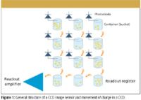
Figure 1
A CCD image sensor has intrinsic noise, including dark, reset, and readout noise. Dark noise is due to variations in dark current, the electrical current produced by thermal agitation of the semiconductor atoms when the image sensor is shielded from light and operating voltages are applied. Dark current in CCDs has been made relatively low by improvements in design. It can be lowered even more by cooling.
The resetting of the charge in each pixel is a large noise source called reset noise. To reduce the reset noise, the amplifier signal is read twice — once with the signal present and once with a reference signal — using a technique called correlated double sampling. Subtracting the two measurements cancels most of the reset noise.
Reducing the reset noise to a negligible value produces an amplifier readout noise of around 5–20 electrons/s, depending upon the quality of the chip. To maintain a low readout noise below 10 electrons, the bandwidth of the readout amplifier must be reduced. This results in reducing the frame rate for a typical 1k × 1k CCD to around 5–10 frames/s. Parallel readout registers can increase the frame rate.
Because the noise sources in a CCD are not correlated, the noise can be calculated from the equation below:
Noise = (Dark Noise2 + Readout Noise2 )1/2
where Dark Noise = (Dark Current × time)1/2 .
For many low-light measurements, the readout noise dominates. However, often users focus on the individual components of the noise instead of the total. This leads some into purchasing a camera with cooling to a very low temperature to reduce the dark current. However, because many experiments are performed with measurement times of just one second or less, an image sensor cooled close to 0 °C is sufficient because the dark noise is much smaller than the readout noise. One exception to this is some types of Raman spectroscopy in which long integration times are required or where a deep depletion CCD is required. The deep depletion CCD has a very high dark current at room temperature and requires cooling down to -100 °C for many Raman measurements.
For single molecule imaging, the readout noise of the CCD becomes a problem because there are so few photons that reach the image sensor. The strategy that has permitted single molecule imaging is the use of EMCCDs (electron multiplication CCDs), which have a gain section in the readout register. A gain as high as 2000 amplifies the signal above the readout noise. The main contributor to the total noise is now the gain noise created by variations in the gain.
CMOS Sensors
The architecture of a CMOS chip differs from the CCD in that there is an amplifier for each photodiode. This is called an active pixel sensor because the amplifier is part of the pixel. Transistor "switches" connect each photodiode to the intrapixel amplifier at the time of readout. The pixel amplifier, switches, and signal lines are masked. This results in a pixel with only about half of the active area. This loss of sensitivity can be largely reversed by adding a microlens array; however, there is a small increase in cost.
Just like the CCD, the CMOS image sensor is read out serially and also has intrinsic noise. Typically the CMOS amplifiers have had much higher readout noise than a CCD. It was also difficult to create identical performance in each amplifier, creating another noise source called fixed pattern noise.
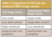
Table I
Dark current for a typical CMOS sensor was also much larger than a CCD. But it was not too much of a problem for the short exposure times of <33 ms that are used in most consumer applications.
The attributes of the CCD image sensor and the CMOS image sensor are summarized in Table I.
Improvements in CMOS Sensors
The continuous improvements driven by Moore's law have created continuous enhancements in both CMOS design and manufacturing technology. This has provided the capability to produce a CMOS imaging device that rivals a front-illuminated CCD. These changes were highlighted in an imaging session called "From the Infrared to X-ray: Advanced Detectors Set to Revolutionize Spectroscopy" presented at the 2009 Pittsburgh Conference.
The two most significant design changes are in the architecture of the active pixel and the readout circuitry. These changes have given the new CMOS sensors lower noise and higher speed.
Improvements in the design and control of the active pixel reduce the noise levels in the new CMOS sensor. By using an optimized buried transistor design, the amplifier noise and the switching noise are reduced. By matching the gain in each amplifier through careful control, the fixed pattern noise is reduced. Failure to match the amplifiers would create the fixed pattern noise that is found in conventional CMOS image sensors.
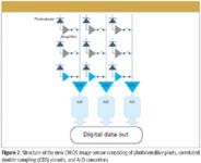
Figure 2
Changes to the readout circuitry allow the new CMOS sensor to achieve higher speed with low readout noise. Unlike the conventional CMOS image sensors, the new designs have parallel readout channels so that as many as 1920 channels are read out in parallel. A correlated double sampling (CDS) circuit is at the output of each channel, followed by an analog-to-digital (A/D) converter (Figure 2). With the massive parallel readout, the signal processing circuits can limit their bandwidth to less than 1 MHz and still attain a fast frame rate of 45 frames/s. Lowering the amplifier bandwidth reduces the readout noise because the contributions from the higher bandwidths are eliminated. Combining the reduced bandwidth, the correlated double sampling, and an A/D converter dedicated to each output results in readout noise of only a few electrons per second without any need to sacrifice the frame rate.
In contrast to a CCD, the readout noise from the CMOS sensor is not a Gaussian distribution, but is asymmetric, as seen in Figure 3. This is because the noise comes from many amplifiers in the CMOS as opposed to only one in the CCD. Reducing the tail of this distribution is another one of the improvements that have been made.
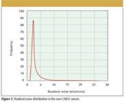
Figure 3
Other developments in the new CMOS sensor include a well capable of storing as many as 18,000 electrons. This well capacity, coupled with a dark current of only a few electrons per second, yields a dynamic range of the analog components (active pixel, amplifier, and CDS circuit) that is well-matched to the 12-bit A/D converters. Some recent CMOS designs use multiple A/D converters for each line to try to attain even higher dynamic range. The dynamic range and the linearity of a camera built with a new CMOS sensor are shown in Figure 4.
Another development is the use of an active pixel configuration with five or three transistors per pixel. Active pixel configurations using up to five transistors are capable of simultaneous capture of the image at the expense of increased dark current and readout noise. This mode of operation is called global shutter. When using three transistors per pixel, only the rolling shutter mode is available (described below).

Figure 4
Readout Methods
The parallel nature of the readout register in the new CMOS sensor creates a unique timing of the image when the CMOS chip is read out at its maximum rate. Each horizontal line is read out in parallel, but displaced by about 15 µs with respect to the previous line. Thus, at 45 frames/s there is a 22 ms delay between the first line and the last line of an image. This readout mode is called rolling shutter. For many applications, rolling shutter does not affect the results.
To increase the readout speed (frame rate) even further, a subarray is often used with a CCD camera. The frame rate is inversely proportional to the number of vertical pixels in the sub-array. The maximum readout rate is limited because all of the data must pass through the single readout amplifier in a CCD. The new CMOS cameras do not have this bottleneck because all of the pixels in one horizontal row are read out in parallel. This allows for some unique high-speed capability.
It is possible to create a square subarray in the new CMOS cameras to increase the frame rate and reduce the size of the image database or to create a rectangular-shaped subarray at much higher speed than an equivalent CCD. For the new CMOS sensor, an array of 8 × 8 or 1920 × 8 can both be read out at 1270 frames/s. For an interline CCD, the readout speed of the square and rectangular subarrays would also be the same. However, the readout rate is much slower compared to the new CMOS sensor. Because many things travel in straight or nearly straight lines, a subarray configuration can be useful for capturing dynamic events such as emission spectra or a protein moving along a microtubule in a cell.
Market Share Based upon Application
A comparison of the CCD image sensor and the new CMOS sensor can be found in Table II.
Table II makes it appear that the new CMOS sensors will replace CCDs in every application. Fortunately for the CCD manufacturers, this is not yet the case. Although CMOS technology has come a very long way in the last few years, CCDs still have some advantages in some applications.
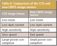
Table II
One of the CCD's advantages is higher sensitivity. Back-thinned CCDs have higher sensitivity in the UV and visible regions than the new CMOS sensors, which are currently not back thinned. For now, the back-thinned CCD's good UV sensitivity makes it more suitable than the new CMOS for spectroscopic applications.
A second advantage is that CCDs can be sensitive to X-rays or NIR, unlike the new CMOS sensor whose sensitivity is currently limited to the visible region (Figure 5). Deep depletion CCDs have the capability to directly detect low energy X-rays. In the 900–1000 nm region, deep depletion CCDs or CCDs with enhanced red sensitivity created by nanostructures are very useful for Raman spectroscopy in the NIR, where autofluorescence from cells is greatly reduced. For these applications, the CCD is still an excellent detector.
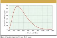
Figure 5
A third advantage of CCDs is the capability for time-delayed integration (TDI), a technique used by instrument manufacturers that are imaging a moving object under low light conditions. In TDI, the CCD control signals move the charge from register to register synchronously with the movement of the object. This increases the signal by the number of pixels that are in the direction of motion. TDI is used to reduce X-ray dosage in a panoramic dental X-ray or to inspect semiconductor wafers at ever faster speeds. The TDI technique is available in CCDs only, not in CMOS image sensors. Because each pixel in a CMOS sensor is connected to the readout amplifier, it is not possible to move the data from pixel to pixel synchronously with the motion of the object.
By contrast, the new CMOS sensors are expected to find many imaging applications. One area that has created a lot of interest is in biology. Cameras are often attached to microscopes to produce quantitative images of fluorescence from an intrinsic protein or from a dye (Figure 6). For example, Ca2+ plays a very important role in cell signaling. Calcium ion fluxes are used to study nerve signal migration. As the electrical signal is transmitted through a neural network, Ca2+ is ejected from each nerve cell. The concentration of calcium in the cell can be monitored with dyes or genetically engineered proteins that change emission wavelength with calcium concentration. Observation of calcium concentrations can be made in single cells or in a section of brain tissue. For both types of experiments, both speed and sensitivity are needed. The high frame rate coupled with the low readout noise of the new CMOS sensors make them candidates for calcium imaging.

Figure 6
Another biological imaging application that requires high sensitivity is total internal reflection fluorescence (TIRF). The sample is placed on a glass slide and illuminated from a very high angle that generates an evanescent wave along the sample side surface of the slide. The properties of the evanescent wave ensure that only molecules within 50 nm of the surface are excited within the sample. This eliminates interference from molecules that reside in the cell interior and allows the biologist to study events such as the excretion of chemotherapeutic agents by drug-resistant cancer cells. Because the excitation layer is very thin, the light level is also low, requiring a sensitive camera.
TIRF traditionally is performed with either a CCD camera or the much more sensitive EMCCD camera whose gain enhances the sensitivity of the camera by amplifying the signal above the readout noise. But TIRF can now be performed using the new CMOS camera with its high sensitivity (the effect of low readout noise). The new CMOS sensor, which has a low readout noise, is expected to replace EMCCDs in a number of applications such as spinning disk confocal microscopy and TIRF microscopy, but not in the most demanding applications such as single molecule detection.
We expect the enhancements in CMOS design and manufacturing that have been discussed to continue creating even better image sensors in the future. Even the current CMOS devices will replace CCDs in many scientific applications and probably create several new applications. However, there will continue to be applications such as TDI that require a CCD.
Ken Kaufmann is VP of Marketing at Hamamatsu Corporation, where he has worked for 25 years. He has a Ph.D. in chemical physics from the Massachusetts Institute of Technology.
