Light-Emitting Diodes
Columnist David Ball discusses the search for light sources that are more energy efficient than incandescent light bulbs. In particular, he focuses on light-emitting diodes.

The development of artificial light sources was a major step forward in technological development. No longer would humanity need to depend upon the sun or relatively dangerous open flames for light. The history of incandescent light bulbs — light sources that depend upon the electrical heating of a thin strip of wire called a filament so hot that it emits substantial amounts of light (and heat) — goes back to the early 1800s and the development of practical batteries. Although several patents were granted around the world for the development of incandescent lights through the 1800s, the first practical incandescent light bulb generally is credited to Thomas Edison, who developed his version in 1879 (Figure 1) (1).

David W. Ball
There are other types of light sources. Fluorescent light bulbs take advantage of a different mechanism for generating light, based more upon quantum-mechanical rules rather than black-body radiation. There are also light sources that are based upon semiconductor constructions called diodes, and so they are more appropriately called light-emitting diodes (LEDs). This column is devoted to these types of lights.
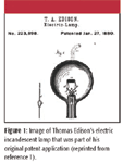
Figure 1
Conductors, Nonconductors, and Semiconductors
The ability of a substance to move charged particles under the influence of an electric potential difference is called the substance's electrical conductivity. The quantity σ, called the conductivity, is the proportionality constant that relates the strength of the potential difference and the induced current density.
Substances that have a high value of σ are called conductors. Most metals, for example, have a high value of σ: for Ag, the most conductive metal, σ has a value of 6.3 × 10⁷ S/m (siemens per meter; a siemen is an inverse ohm, or Ω–1 ). Substances that have a low value of σ are called nonconductors. The conductivity of glass ranges from 10–10 –10–14 S/m, whereas polytetrafluoroethylene (Teflon) has a σ of 10–22 –10–24 S/m. Another word for nonconductor is insulator.
Because all substances have values of conductivity, the difference between a conductor and a nonconductor is a matter of degree. On a table of conductivities, substances that are obvious conductors are separated by substances that are obvious nonconductors around σ ≈ 1, but that is a fluid boundary.
A semiconductor has electrical conductivity properties between those of conductors and nonconductors. Given what we said about the difference in the values of σ for conductors and nonconductors, being a semiconductor is also a question of degree. We can propose values of σ ranging from 10 to 1 × 10⁻³ S/m as characteristic of semiconductors, but these values are not set in stone. Nonetheless, intermediate values of σ characterize semiconductors.
Another way to describe conductors and nonconductors is in terms of band gap. Imagine that all of the electrons in a solid have a particular range of energies. This range of energies is called the valence band. Now imagine that an electron has to be promoted to a higher range of energies to be free enough to conduct electricity. This higher range of energies is called the conduction band. The energy difference between the valence band and the conduction band is called the band gap. Insulators have a relatively high band gap (Figure 2a), on the order of 300 kJ/mol. Semiconductors have a small band gap (Figure 2b), so that either temperature can excite electrons thermally or the presence of dopants can provide excess electrons or holes that would have an energy in the conduction band. In conductors (Figure 2c), the band gap is zero and the two bands overlap.
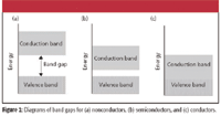
Figure 2
Many semiconductors are based upon the element silicon. However, pure silicon is, in fact, a nonconductor. In their pioneering work, Pearson and Bardeen (2) estimated that the electrical conductivity of pure Si was about 1 × 10⁻⁴ S/m, just outside of our arbitrary range for semiconductors and into nonconductor territory.
Despite being a nonconductor in its pure state, silicon has another property that is very useful: impure silicon has highly variable electrical conductivities. Thus, by varying the type and amount of impurity, we can manufacture impure silicon with a range of electrical properties, mostly in the semiconductor range of σ. These intentional impurities are called dopants, and the process of intentionally adulterating silicon is called doping. (Substances other than silicon can form the basis for semiconductors, including germanium, silicon carbide, and various transition metal oxides and sulfides. Here, we will focus on silicon as the basis for semiconductors.)
There are two general ways of doping silicon to make a semiconductor. In the pure element, silicon makes four covalent bonds to other silicon atoms in a three-dimensional, diamond-like structure. A two-dimensional diagram of pure silicon is shown in Figure 3a. Suppose that a small amount (10–2 –10–7 %) of an element like boron were added to pure silicon as a dopant. Neutral boron typically only makes three covalent bonds, so one of the valence electrons on an adjacent silicon atom is unbonded, and there is a "hole" on the boron atom (Figure 3b). Electrically, that hole acts as the opposite of an electron, so we can pretend it has a positive charge, even though the sample is still electrically neutral. Because of the presence of the hole, the conductivity of this doped sample of silicon is higher than that of pure silicon — it is now a semiconductor. Because of the presence of "positively charged" holes, it is more accurately called a p-type semiconductor. (Blue diamonds, like the Hope diamond, are natural p-type semiconductors. The carbon lattice has been "doped" with boron atoms.)

Figure 3
Suppose an element such as phosphorus were added to pure silicon as a dopant. Neutral phosphorus typically likes to make five bonds, but in a normal silicon lattice there are only four next-nearest neighbors with which to make covalent bonds. One of the valence electrons in the phosphorus atom is unbonded, as shown in Figure 3c. Because of the presence of the extra unbonded electron, the conductivity of this doped silicon is also higher than that of pure silicon, and it too is a semiconductor. This type of doped silicon is called an n-type semiconductor.
Diodes
A diode is an electronic component that allows current to travel in one direction but not in the other direction. The earliest diodes were known colloquially as vacuum tubes. Figure 4 shows a diagram of a vacuum tube. It is essentially a glass envelope with a vacuum inside (residual pressure of about 10–10 –10–13 atm) and several pieces of metal strips or wires called electrodes. The cathode is negatively charged and near a heater. The heater warms up the cathode, and when hot, the cathode thermally emits electrons (a process called thermionic emission). The other electrode, the positively charged anode, attracts the emitted electrons, and current flows from cathode to anode. If the current polarities were switched, however, electrons (that is, current) would not flow because the anode does not have a heater nearby to cause thermionic emission. Thus, in a vacuum tube, electric current flows in only one direction. A vacuum tube also takes time to operate, because the heater has to warm up the cathode before electron emission occurs. This is why older electronics based upon vacuum tubes had a lag time before operating properly.
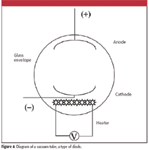
Figure 4
Diodes also can be made from semiconductors. Figure 5 is a diagram of a simple semiconductor diode. It is essentially two pieces of semiconductor, one p-type and one n-type, in contact. The very thin region about the contact surface is called the depletion zone. In this zone, the electron-deficient matter in the p-type semiconductor and the electron-rich matter in the n-type semiconductor essentially cancel each other out, so the depletion zone is relatively nonconducting.

Figure 5
How does this diode work? Consider the two ways in which a semiconductor diode can be connected to a source of electricity. In one case, the positive end of a circuit can be connected to the p-type semiconductor and the negative end of the circuit can be connected to the n-type semiconductor. This type of connection is called forward-biased and is shown in Figure 6a. This type of connection essentially increases the number of electrons in the n-type semiconductor and decreases the number of electrons in the p-type semiconductor — that is, it increases the number of holes in the p-type semiconductor. The net effect is to reduce the width of the depletion zone. Eventually, the depletion zone gets so narrow that electrons can jump across the barrier, and current flows. Usually, some minimum voltage is needed to narrow the zone enough so that current flows; for silicon diodes, this minimum voltage is about 0.6–0.7 V.
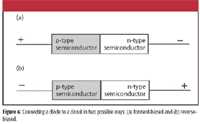
Figure 6
In the second case, the negative end of the circuit is connected to the p-type semiconductor, and the positive end of the circuit is connected to the n-type semiconductor. This is shown in Figure 6b and is called reverse-biased. Putting electrons into the p-type semiconductor has the effect of pulling holes toward the circuit, and vice versa in the n-type semiconductor. This has the net effect of increasing the size of the depletion zone, decreasing the chance that electrons will pass from one side of the diode to the other. Thus, current is impeded and does not flow in that configuration. (There is a limit, however — if the potential across the depletion zone goes too high, the diode will essentially short out and current will flow. Diodes that are designed to do this at a specific voltage are called Zener diodes.)
LEDs
In the course of operating diodes, as an electron and a hole come together, energy is given off. In many cases, the energy goes into solid-state vibrational modes, or phonon modes, of the semiconductor. This is, in fact, what happens in most silicon-based diodes.
In other cases, as electron–hole combinations occur, the energy is given off as a photon of light. These cases are called LEDs (Figure 7). For a photon to be given off, the maximum energy of the valence band must correspond to the minimum energy of the conduction band in momentum space; if they are too far away, an electron has to change its momentum by interacting with the phonon modes of the solid semiconductor, which inhibits photon emission. Such is the case with most silicon-based diodes. However, diodes made with other materials, like gallium arsenide, gallium phosphide, zinc sulfide, and mixed aluminum-indium-gallium phosphides, have appropriately located valence and conduction bands, so as electrons are pushed through the depletion zone of the diode, light is emitted as the electrons encounter holes and release energy.

Figure 7
Unlike a laser, the light emitted from an LED is not monochromatic. However, the range of wavelengths given off by an LED can be rather narrow, as little as 25 nm. As such, the light given off by an LED is fairly pure in color. As might be expected, the color of light emitted depends upon the energy difference between the valence and conduction bands. Low energy differences yield infrared or red diodes, with higher band gaps providing higher-energy light. Higher-energy light provides a challenge, however; the higher the band gap, the more a solid tends toward being an insulator, not a semiconductor. However, in the early 1990s, solid-state techniques were developed to allow the production of reliable blue- and ultraviolet-emitting diodes.
White-light diodes also are available, but they are not full-spectrum white lights. Rather, they are blue LEDs covered by a cerium-doped yttrium aluminum garnet (Ce:YAG). The Ce:YAG phosphoresces yellow when the diode emits blue light, and the combination of blue and yellow light is perceived by the eye as "white."
LEDs also can be configured as lasers. Interested readers are directed elsewhere for additional information. Laser diodes have two major differences from other lasers. They are, again, not monochromatic; and because of their physical construction, the emitted light is not well collimated. Despite this, laser diodes are actually the most popular form of laser produced today. Barcode readers at the grocery store and laser pointers in the lecture hall use laser diodes. Compact disc players, CD-ROM devices, DVD players, and laser printers use laser diodes as well. Given the prevalence of such devices in our society, it is easy to realize that the population of LEDs of all sorts is very high, indeed.
David W. Ball is a professor of chemistry at Cleveland State University in Ohio. Many of his "Baseline" columns have been reprinted in book form by SPIE Press as The Basics of Spectroscopy, available through the SPIE Web Bookstore at www.spie.org. His most recent book, Field Guide to Spectroscopy (published in May 2006), is available from SPIE Press. He can be reached at d.ball@csuohio.edu his website is academic.csuohio.edu/ball.
References
(1) US Patent No. 223898. From the US Patent and Trademark Office website, www.uspto.gov. Accessed June 13, 2007.
(2) G.L. Pearson and J. Bardeen, Phys. Rev. 75, 865 (1948).
New Study Reveals Insights into Phenol’s Behavior in Ice
April 16th 2025A new study published in Spectrochimica Acta Part A by Dominik Heger and colleagues at Masaryk University reveals that phenol's photophysical properties change significantly when frozen, potentially enabling its breakdown by sunlight in icy environments.