Mid-IR Luminescence of Nanocrystalline II-VI Semiconductors Doped with Transition Metal Ions
A novel method of transition metal (TM) (Cr, Co, and Fe)-doped nanocrystals fabrication based upon laser ablation was demonstrated. For the first time, mid-IR luminescence from TM:II-VI nanocrystals was reported.

Middle-infrared (mid-IR) laser sources operating over a "molecular fingerprint" 2–15 μm spectral range are in great demand for a variety of applications including molecular spectroscopy, noninvasive medical diagnostics, industrial process control, environmental monitoring, atmospheric sensing and free space communication, oil prospecting, tracking of naturally occurring gas emitters — methane seeps and volcanoes — and numerous defense-related applications such as infrared countermeasures, monitoring of munitions disposal, and standoff detection of explosion hazards. Mid-IR wavelengths usually are generated using relatively complex nonlinear optical conversion techniques or by means of direct generation in heterojunction lead-salt, antimonite, or quantum cascade semiconductor lasers featuring limited output power and tuning range.
Impurity-doped crystalline vibronic lasers having a gain bandwidth up to 50% of the central wavelength represent another viable route for broadly tunable mid-IR coherent sources. Among them, transition metal (TM) (TM2+ , such as Cr2+ or Fe2+)–doped binary and ternary chalcogenide crystals represent a relatively new class of solid-state gain media with strong and ultrabroad absorption and emission bands in the mid-IR range of optical spectra. In 1996, scientists from the Lawrence Livermore National Laboratory (1) were the first to show that among different types of crystalline gain materials, TM2+-doped wide bandgap II–VI semiconductor crystals could be very special for mid-IR lasing. Active interest in TM-doped II–VI compounds inspired by this research was explained by the fact that these media are close mid-IR analogs of the titanium-doped sapphire (Ti-S) in terms of spectroscopic and laser characteristics, and it was anticipated that TM2+-doped chalcogenides will lase in the mid-IR with a great variety of possible modes of oscillation, similar to the Ti-S laser. Indeed, optically pumped room-temperature lasers based upon Cr:ZnS, Cr:ZnSe, Cr:Cd1–xMnxTe, Cr:CdSe, and Fe:ZnSe crystals providing access to the 2–5 μm spectral region with high (up to 70%) efficiency, multi-watt-level output powers, tunability in excess of 1000 nm, and narrow spectral linewidth (<20 MHz), have been reported by several groups (2,3). Arguably these lasers represent the simplest and most cost-effective light sources in this 2–5 μm wavelength range.
In addition to effective room-temperature mid-IR lasing, TM-doped II–VI media, being wide-band semiconductors, hold potential for direct electrical excitation. Two promising routes for achieving TM:II–VI mid-IR lasing under electrical excitation were envisioned: utilization of TM-doped quantum well II–VI heterostructures, and utilization of thin films based upon TM-doped nanocrystals, or nanocrystals dispersed in a conductive matrix (4). In both cases, quantum confinement enables an efficient energy transfer from the host to the active transition metal (Cr or Fe) impurity. It was verified experimentally for Mn2+:ZnS nanocrystals (5–7) and qualitatively explained by the increase of the oscillator strength of the exciton bound to the impurity center. The idea of achieving the goal of electrically pumped mid-IR semiconductor lasers based upon TM-doped quantum confined structures was reported (4,8,9), and first steps were performed by studying bulk mid-IR electroluminescence of Cr (4,10,11) and Cr excitation and lasing via photoionization transitions (4,12). Here, we describe our first steps toward fabrication and spectroscopic characterization of TM-doped nanocrystals.
Preparation of II–VI Semiconductor Nanocrystals Doped with TM Ions
The majority of methods of metal and semiconductor nanocrystal synthesis are based upon chemical approaches in which a variety of functional groups are used to stabilize nanocrystals and serve as capping agents. Various byproducts of chemical reactions can also interact with nanocrystals, and their removal from the surface is tricky. Even small amounts of residual organic molecules used in nanocrystal synthesis might reabsorb or quench nanocrystal luminescence in the IR region.
An entirely physical approach for the fabrication of metal and semiconductor nanocrystals, such as laser ablation, enables formation of pure uncapped nanocrystals. Laser ablation in a liquid environment has been used for the fabrication of semiconductor and metal nanoparticles (13,14). However, formation of semiconductor nanocrystals doped with TM ions under laser ablation has not been documented.
TM- (Cr, Co, and Fe) doped II–VI (ZnS, ZnSe) semiconductor nanocrystals were prepared by laser ablation in a liquid environment in several steps. Initially, chemical vapor deposition (CVD)–grown polycrystalline ZnS and ZnSe samples placed in evacuated and sealed quartz ampoules were subjected to 7–10 days of postgrowth thermo-diffusion of TM ions from the metal phase at 970 °C. The detailed description of the process can be found elsewhere (15). The average TM ions concentration was 1018 –1019 cm–3.
Nanocrystals were prepared by ablation of bulk polycrystalline TM-doped ZnS and ZnSe samples in double-distilled, deionized water with a radiation of the fundamental harmonic of Nd:YAG laser with 30-ps pulse duration, 10-Hz repetition rate, and pulse energy of 10 mJ. The laser radiation was focused to a spot size of approximately 1 mm. Uncapped nanocrystals quickly aggregated and formed precipitate. Precipitated nanocrystals were collected and dried under ambient conditions for X-ray diffraction (XRD) and spectroscopic studies.
At the last stage of nanocrystal preparation, their suspension in a quartz spectroscopic cell was illuminated additionally by the radiation of the third harmonic (355 nm) of a picosecond Nd:YAG laser with pulse energy of 15 mJ. The laser beam was not focused and had ~1 cm diameter. Initially cloudy colloidal suspension became clear after 10 min of irradiation, which indicates the formation of smaller particles. The prepared nanocrystals tend to form aggregates and precipitate in several hours. Precipitated aggregates were collected and dried under ambient conditions.
Dry nanocrystals were evenly dispersed on microscope slides for XRD measurements or kept in a quartz cell for spectroscopic studies.
XRD Characterization of II–VI Nanocrystals Doped with TM Ions
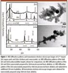
The crystalline grain size and structure of nanocrystals was studied by XRD using θ–2θ angle mode of diffractometer with a Cu K-alpha anode. The XRD spectra depicted in Figure 1 correspond to Cr-doped ZnS and ZnSe polycrystalline samples as well as nanocrystals prepared from the bulk samples by laser ablation. Initial bulk polycrystalline ZnS and ZnSe samples had a zinc-blend structure, as seen in Figure 1a. The most prominent ZnS diffraction peaks located at 2θ = 28.6, 33.2, 47.6, and 56.5° coincide with (111), (200), (220), and (311) planes reflections of the zinc-blend structure. Similarly, the ZnSe polycrystalline target had XRD peaks at 2θ = 27.5, 45.5, and 53.3° corresponding to (111), (220), and (311) planes reflections of cubic ZnSe.

Figure 1
As shown in Figure 1b, the nanocrystals fabricated by 1064-nm laser ablation also featured several additional peaks characteristic to wurtzite structure. Specifically, Cr2+:ZnS nanocrystals exhibit XRD pattern (Figure 1b) with several wurtzite ZnS (100), (101), (102), and (103) peaks. The other peaks of the wurtzite structure (002), (110), and (112) overlap with main peaks of the zinc-blend structure (111), (220), and (311). Similar results were obtained for Cr2+:ZnSe nanocrystals. This indicates that the ZnS and ZnSe nanocrystals prepared by laser ablation had mixed wurtzite and zinc-blend structures.
XRD peaks of nanocrystals obtained after additional ultraviolet irradiation exhibit significant broadening, indicating the particle's size reduction. The mean nanocrystal size can be calculated from the width of XRD peaks using Scherrer's equation, D = kλ/Bcos(2θ), where λ = 0.154 nm is X-ray wavelength, 2θ is diffraction angle, B is a measured full width half maximum (FWHM) of the peaks, and k = 0.9. The average size of the Cr2+:ZnS nanocrystals was 11 nm before and 3 nm after the UV treatment. Similarly, Cr2+:ZnSe nanocrystals have a size of 13 nm before the UV treatment. However, a prolonged UV treatment of ZnSe nanocrystals results in sample degradation. The size of nanocrystals fabricated by a single-stage 1064-nm laser ablation and estimated from the XRD measurements was consistent with the transmission electron microscope images of nanocrystals depicted in Figure 1.
Spectroscopic Characterization of II–VI Nanocrystals Doped with TM Ions
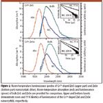
5D term is the ground state of free Cr2+ (3d4) ions. This state is split in a weak tetragonal Td crystal field of the II–VI crystals into the ground 5T2 and excited 5E states. The spectral range of the 5T2 5E spin-allowed transitions in Cr2+-doped chalcogenides spans over 1.5–3.5 μm. The broad absorption bands of the Cr2+ ions in ZnS and ZnSe are centered at 1680 and 1780 nm, respectively, and feature FWHM of ~400 nm (Figure 2).

Figure 2
Room-temperature photoluminescence spectra of Cr2+:ZnS and Cr2+:ZnSe nanocrystals are demonstrated in Figure 2. The photoluminescence was excited by the 5 ns radiation of an optical parametric oscillator operating near the absorption maxima, and photoluminescence spectra were measured by IR spectrometer-InSb detector-boxcar integrator combination. The photoluminescence spectra of Cr-doped bulk crystals obtained at the same experimental conditions are also shown for comparison in Figure 2. The photoluminescence bands of Cr-doped ZnS and ZnSe nanocrystals are not only blue-shifted with respect to the photoluminescence of bulk polycrystalline samples, but they also have a different shape with a strong photoluminescence signal suppression at wavelengths longer than 2600 nm. The blue shift of the Cr-doped nanocrystals photoluminescence maxima can be attributed to the increase of the strength of the crystal field resulting in larger splitting between the ground 5T2 and excited 5E states of Cr in nanocrystalline environment, while the most probable factor affecting the shape of Cr2+:ZnS and ZnSe nanocrystals photoluminescence spectra is emission reabsorption by OH groups possibly remaining on the nanocrystal surface.
The photoluminescence kinetics of Cr2+:ZnS and Cr2+:ZnSe nanocrystals are depicted in Figure 2 as inserts. The room-temperature luminescence lifetime of Cr2+:ZnS nanocrystals was 2.6 μs, which is noticeably shorter than the 6 μs lifetime typical of Cr2+ in the bulk crystals. However, the Cr2+:ZnS nanocrystals' lifetime was 5 μs at 77 K, which is close to that of the bulk samples. It is probable that the shortening of the Cr2+ excited-state lifetime in ZnS nanocrystals at room temperature with respect to the bulk samples is due to Cr2+ photoluminescence quenching by the surface states and OH groups. On the other hand, a smaller spectral overlap of Cr2+ photoluminescence and OH absorption at 77 K mitigates this quenching. Similar results were obtained for Cr2+:ZnSe nanocrystals photoluminescence lifetime behavior.
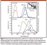
The absorption and photoluminescence spectra of Co2+:ZnSe polycrystalline bulk samples as well as photoluminescence of Co2+:ZnSe nanocrystals are shown in Figure 3. The ground level 4F of a free Co2+ (3d7) ion is split by the crystal field into three levels: 4T1, 4T2, and 4A2. The absorption spectra of Co2+-doped II-VI bulk crystals typically have two bands associated with 4A2→4T1 (~1500 nm) and 4A2→4T2 (~3000 nm) transitions (1). The 4A2→4T2 transition is relatively weak because it is symmetry-forbidden (1). 4T2→4A2 room-temperature luminescence spectra of Co2+:ZnSe nanocrystal and bulk samples excited via 4A2→4T1 transition (1600 nm) are shown in Figure 3. One can see from Figure 3 that the photoluminescence signal of Co2+:ZnSe nanocrystals is strongly suppressed at 2800 nm compared with the bulk sample emission, which can be attributed to light reabsorption by OH groups remaining at the surface of the nanocrystals. Indeed, the insert in Figure 3 demonstrates that the room-temperature luminescence lifetime of Co2+:ZnSe nanocrystals is 160 μs, which is practically twice smaller than the 290 μs photoluminescence lifetime featured by the bulk sample. It is noteworthy that Co2+:ZnSe nanocrystals' photoluminescence lifetime increased and became comparable with that of a bulk sample when nanocrystals were dried using anhydrous alcohol. This fact is in agreement with the hypothesis of OH groups affecting emission properties of Cr- and Co-doped ZnS and ZnSe nanocrystals. It also indicates that the number of OH groups can be reduced and thus, parasitic nonradiative relaxation of excited Cr and Co ions can be mitigated by the application of an appropriate nanocrystal drying procedure.

Figure 3
The energy structure of the Fe2+ ions (3d6) is similar to the Cr2+ (3d4), and according to the Hund's rule, 5D is a ground term. The ground state in the tetrahedral crystal field of the II–VI crystals is split into doublet 5E and triplet 5T2. However, in contrast to the chromium ions, the lowest level of the iron is doublet 5E. The energy splitting of Fe2+ ions is smaller compared to chromium ions, and as a result, the iron absorption and emission bands usually are shifted to the longer wavelength. Recently, a room-temperature lasing of Fe:ZnSe tunable over the 3.77–5.05 μm spectral range was demonstrated (16,17). For these low-energy mid-IR transitions, the major factor limiting photoluminescence efficiency is nonradiative quenching of the excitation. Remarkable differences in thermal quenching of Mn2+ ion photoluminescence in nanocrystal and bulk ZnS material were revealed by Tanaka (7), where an increased quantum efficiency of Mn2+:ZnS nanocrystal photoluminescence was explained by a weaker electron-phonon coupling in the nanocrystals. Hence, it is of interest to study whether, similarly to Mn in ZnS, the thermal quenching of Fe2+:ZnSe nanocrystals can be mitigated and whether one can obtain broadband room-temperature mid-IR photoluminescence with wavelengths longer than 4 μm. The absorption and photoluminescence spectra of iron-doped ZnSe bulk and nanocrystal samples are depicted in Figure 3. The Fe2+:ZnSe room-temperature absorption spectrum features an ultrabroad band spanning over 2.5–4.5 μm. Room-temperature luminescence of Fe2+:ZnSe nanocrystals and bulk material under excitation by the 2.8-μm radiation of Er:Cr:YSGG laser is also depicted in Figure 3. As one can see, at room temperature, Fe2+:ZnSe nanocrystals have a broadband (3.5–5.2 μm) luminescence practically identical to Fe2+:ZnSe bulk photoluminescence with a characteristic dip at 4.25 μm caused by absorption of atmospheric CO2.
Conclusion
TM-doped II–VI media hold the potential for lasing at room temperature under direct electrical excitation. These studies demonstrate the initial effort toward achieving this goal by studying Cr2+-, Co2+-, and Fe2+-doped nanocrystals. We have demonstrated a novel method of TM-doped II–VI nanocrystal production by laser ablation in a liquid environment. This method enables fabrication of II–VI nanocrystals doped with a variety of TM ions using laser ablation of thermodiffusion-doped polycrystalline targets. This method has a significant advantage over chemical methods because of its simplicity and the absence of residual organic molecules on the nanoparticles' surface. For the first time, to our knowledge, TM-doped II–VI nanocrystals demonstrated strong mid-IR luminescence. This technology opens new pathways for future development of optically and electrically pumped mid-IR lasers based upon TM-doped quantum confined structures.
Acknowledgments
This material is based upon work supported by the National Science Foundation under Grants No. ECS-0424310, EPS-0447675, and BES-0521036.
C. Kim, D.V. Martyshkin, V.V. Fedorov, I.S. Moskalev, and S.B. Mirov are with the Department of Physics, University of Alabama at Birmingham, Birmingham, AL.
References
(1) L.D. DeLoach, R.H. Page, G.D. Wilke, S.A. Payne, and W.F. Krupke, IEEE J. Quantum Electron. 32, 885–895 (1996).
(2) I.T. Sorokina, Opt. Mat. 26(4), 395–412 (2004).
(3) S. Mirov, V. Fedorov, I. Moskalev, and D. Martyshkin, IEEE J. Sel. Topics Quantum Electron. 13(3), 810 (2007).
(4) V.V. Fedorov, A. Gallian, I. Moskalev, and S.B. Mirov, J. Lumin. 125, 184–195 (2007).
(5) R.N. Bhargava, D. Gallagher, X. Hong, and A. Nurmikko, Phys. Rev. Lett. 72(3), 416–419 (1994).
(6) R.N. Bhargava, J. Crystal Growth 214/215, 926–930 (2000).
(7) M. Tanaka, J. Lumin. 100, 163–173 (2002).
(8) S.B. Mirov, V.V. Fedorov, K. Graham, I.S. Moskalev, I.T. Sorokina, E. Sorokin, V. Gapontsev, D. Gapontsev, V.V. Badikov, and V. Panyutin, in 5th International Conference on Mid-Infrared Optoelectronic Materials and Devices, Annapolis, MD, Sept. 8–11, 2002, Abstract Book pp. 143-144.
(9) A. Gallian, V.V. Fedorov, J. Kernal, J. Allman, S.B. Mirov, E.M. Dianov, A.O. Zabezhaylov, and I.P. Kazakov, Appl. Phys. Lett. 86, 091105 (2005).
(10) L. Luke, V.V. Fedorov, I. Moskalev, A. Gallian, and S.B. Mirov, in Solid State Lasers XV: Technology and Devices, H.J. Hoffman, R.K. Shori, Eds., Proc. Of SPIE Vol. 6100 (SPIE, Bellingham, Washington, 2006), 61000Y-1-8.
(11) J. Jaeck, R. Haidar, E. Rosencher, M. Caes, M. Tauvy, S. Collin, N. Bardou, J.L. Pelouard, F. Pardo, and P. Lemasson, Opt. Lett. 31, 3501–3503 (2006).
(12) A. Gallian, V.V. Fedorov, J. Kernal, S.B. Mirov, and V.V. Badikov, in Advanced Solid State Photonics 2005 Technical Digest on CD-ROM (The Optical Society of America, Washington, DC, 2005), MB12.
(13) K.V. Anikin, N.N. Melnik, A.V. Simakin, G.A. Shafeev, V.V. Voronov, and A.G. Vitukhnovsky, Chem. Phys. Lett. 366, 357–360 (2002).
(14) T. Sadaki, Y. Shimizu, and N. Koshizaki, J. Photochem. Photobiol., A 182, 335–341 (2006).
(15) S.B. Mirov, V.V. Fedorov, K. Graham, I.S. Moskalev, I.T. Sorokina, E. Sorokin, V. Gapontsev, D. Gapontsev, V.V. Badikov, and V. Panyutin, IEE Optoelectronics 150(4), 340–345 (2003).
(16) J. Kernal, V.V. Fedorov, A. Gallian, S.B. Mirov, and V. Badikov, Optics Express 13(26), 10608–10615 (2005).
(17) V.V. Fedorov, S.B. Mirov, A. Gallian, D.V. Badikov, M.P. Frolov, Y.V. Korostelin, V.I. Koslovsky, A.I. Landman, Y.P. Podmar'kov, V.A. Akimov, and A.A. Voronov, IEEE J. Quantum Electron. 42(9), 907–917 (2006).

AI Shakes Up Spectroscopy as New Tools Reveal the Secret Life of Molecules
April 14th 2025A leading-edge review led by researchers at Oak Ridge National Laboratory and MIT explores how artificial intelligence is revolutionizing the study of molecular vibrations and phonon dynamics. From infrared and Raman spectroscopy to neutron and X-ray scattering, AI is transforming how scientists interpret vibrational spectra and predict material behaviors.
Real-Time Battery Health Tracking Using Fiber-Optic Sensors
April 9th 2025A new study by researchers from Palo Alto Research Center (PARC, a Xerox Company) and LG Chem Power presents a novel method for real-time battery monitoring using embedded fiber-optic sensors. This approach enhances state-of-charge (SOC) and state-of-health (SOH) estimations, potentially improving the efficiency and lifespan of lithium-ion batteries in electric vehicles (xEVs).
New Study Provides Insights into Chiral Smectic Phases
March 31st 2025Researchers from the Institute of Nuclear Physics Polish Academy of Sciences have unveiled new insights into the molecular arrangement of the 7HH6 compound’s smectic phases using X-ray diffraction (XRD) and infrared (IR) spectroscopy.