Raman Images from Raman Maps - Spatial Resolution, Mapping Speed, and Multivariate Techniques for Constructing the Image
Columnist Fran Adar discusses the physical determinants of spatial resolution and developing methods to improve the mapping speeds of Raman images.

The spatial resolution of any imaging tool is determined by diffraction theory. In an optical microscope, it is assumed that a microscope objective is illuminated uniformly by light and the focal area is described by the Airy disk as
ωo = 1.22 (λ/NA)
where NA stands for the numerical aperture of the objective. When the same objective is used to focus a laser beam, the beam profile is not uniform (it is very often Gaussian), nor does it fill the objective aperture. However, the minimum beam spot is described by a similar expression:
ωo = K (λ/NA)
with the constant K not very different from 1. That means that for laser lines in the visible part of the spectrum (approximately 0.5 μm) and for high-magnification objectives (for example 90× with NA = 0.9), the minimum spot size is near 0.68 μm. The question, of course, is how to measure the spot. One method has been to perform a line profile across a silicon–metal interface: Follow the silicon signal as the sample is moved so that the metal masking the silicon falls under the laser-illuminated spot, then take the derivative of the intensity profile of the silicon, and measure the full width at half maximum (FWHM). We will show results of polysilicon lines on silicon done at several laser wavelengths, but first we want to show a Raman image of particles with submicrometer dimensions.

Fran Adar
A sample that was known to have particles of diamond with diameters of 0.2 μm (200 nm) or larger was mapped with the HeNe laser (632.8 nm). For this sample, Raman maps should be acquired with steps of about 40 nm (five points per particle), but a stage with only 100-nm (0.1-μm) steps was available. The result, shown in Figure 1, was an image of a particle whose FWHM was no greater than 0.4 μm! Because this quantity represents a convolution of the beam profile and the particle size, which was 0.2 μm, the beam profile must be somewhere in the range of 0.2 to 0.3 μm, considerably smaller than the prediction from diffraction theory.
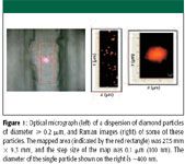
Figure 1
Additional experiments were done on polymer particles. First we systematically compared the images obtained by varying the step size between data points for a given particle. Figure 2 shows the results obtained from maps of a 6-μm bead of polystyrene obtained with 1.0-, 0.5-, and 0.1-μm steps. Clearly, 1-μm steps are far from adequate to map out a particle 6 μm in diameter.
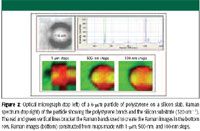
Figure 2
In the past, it was conventional (and conservative) to say that the spatial resolution of the Raman microscope is about 1 μm. It is clear that the technology does much better than that. How else can it be tested? What would happen if we looked at polymer beads of different chemical composition? The next experiment to be tested was to acquire maps of 1-μm beads of a mixture of polystyrene and polymethylmethacrylate. In spite of the fact that polymers often do not like to mix, it was possible to identify a region with beads of the two components. Figure 3a shows a layer of close-packed spheres, with a highlighted rectangular area where Raman mapping was performed. Figure 3b shows the Raman map constructed from the factor loadings generated from multivariate analysis.
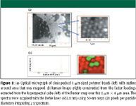
Figure 3
What can this Raman image tell us about the spatial resolution of the measurement? Clearly, the morphology of the spheres is well replicated. But what about the contrast in the image? Consider two line profiles extracted from this image — one taken across two like particles, and one across two dissimilar particles. Figure 4 shows the Raman image with two lines, indicating the track over which line profiles were extracted. When the track traversed the green beads, the profile shows a double hump and the width of the beads would be determined by bandfitting. This profile looks like that used to define the Rayleigh criterion for detection of two particles. On the other hand, when the track traversed beads of different chemistries, one does not have to define or invoke any mathematical definition to determine the bead size. It would be measured directly as the FWHM of the profile, and perhaps more importantly, the contrast is high. In summary, the difference in chemistry provides contrast in the chemical image that is not possible in a standard microscopic image.
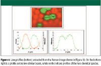
Figure 4
What role does the laser wavelength play in this? It is well known that the diffraction limit is wavelength dependent. What do the measurements show? Now we will look at line profiles of the frequency of polysilicon lines deposited on silicon. Figure 5 shows micrographs of the lines.
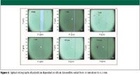
Figure 5
Polysilicon is the polycrystalline form of silicon. The Raman spectrum is very similar except that the Raman band tends to appear at lower frequency, and is sometimes broadened relative to that of single-crystal silicon. Therefore, the only way that contrast can be produced is to plot either the frequency or the line width in the profile. The following results will be a plot of the Raman frequency of the silicon as the sample was rastered under the laser beam. Measurements were made at 633, 532, and 325 nm. In addition to recognizing the role of the wavelength in determining the diameter of the laser spot, it is important to recognize that the depth of penetration exhibits significant dependence on the wavelength. The three lasers penetrate about 3 μm, 0.7 μm, and 10 nm into the silicon. Figure 6 shows the results for the 633-and 532-nm lasers from the 10-and 1-μm lines.
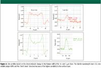
Figure 6
On the 10-μm line, the HeNe (633-nm) laser penetrates far more than the 532-nm laser, so the frequency shift represents more of an average of the polysilicon at the surface and the substrate material. Therefore, the line shift is considerably less than for the 532-nm laser. The profile of the 10-μm line taken with the 532-nm laser shows the typical "bird's beak" due to higher stress at the edges of the line. On the 1-μm line of polysilicon, the FWHM of the 532-nm profile is slightly narrower than that of the 633-nm line, presumably due to the smaller diffraction limit at that wavelength. The larger band shift with this laser wavelength again is due to the higher sensitivity to the surface material. While these results are interesting and meaningful, things really become interesting in the measurements done at 325 nm.
Line profiles generated with the 325-nm light for all the polysilicon lines are shown in Figure 7. In these measurements, the edge effects at the edges of the lines are more pronounced than what was observed with the visible laser lines because only the top 10-nm layer is being probed. For the purposes of this column, the most important result is the measured FWHM of the 0.2-μm polysilicon line, which was measured to be about 0.3 μm, less than the Airy-disk-predicted diffraction-limited spot size of 0.45 μm!
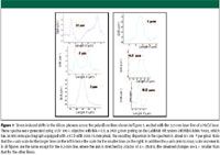
Figure 7
New Methods for Collecting Raman Maps
Raman imaging provides new capabilities to the microscopist: chemical contrast and spatial resolution that might be a bit better than the predictions of the diffraction-limit. But speed is still an issue. What has been done to increase the speed of the spectral acquisition?
CCD Readout
The Raman microscopes have now been designed to take full advantage of all the photons available. If there is enough signal in an acquisition of 10–100 ms, it then becomes quite inefficient to spend tens to hundreds of milliseconds to read the CCD, transfer the signal to the computer, and start and stop the XY stage that rasters the sample. The solution to this bottleneck is to synchronize motion of the XY stage with the CCD readout. In addition, it is possible to use new CCD chips, which have storage areas so that one frame can be transferred to the storage area, and while its charges are being digitized and transferred to the computer, the next frame is being integrated.
Laser Scanning
A newly developed method for scanning a confocal beam across the sample (DuoScan imaging system, HORIBA Jobin Yvon, Edison, New Jersey) has several applications. In this device, two scanning mirrors mounted above the microscope nosepiece move a diffraction-limited spot across the sample. A 50× long working distance objective can provide a spot as large as 30 μm while maintaining the advantages of high collection efficiency and high depth resolution of high-NA objectives. This can be useful in mapping pharmaceutical tablets or geological specimens, where the sample features are greater than 5 μm. But, in addition, the scanning of the mirrors can be used to provide step sizes in the Raman maps as small as 10 nm. If the Raman microscope measurements discussed earlier are demonstrating spatial resolution of 300 nm or better, then for some applications, it might be sensible to record maps with step sizes in the tens of nm range.
It is probably useful to make a final comment regarding the spectral signal-to-noise ratio (S/N) in a map. As spectroscopists, we tend to want to record spectra with high S/N. What often is not recognized is that a map with a very large number of spectra often can produce a high quality image even though the individual spectra are noisier than what we might be used to. This is because the spectra tend to classify into groups determined by the systematic features, not the random noise.
Summary
Raman maps that show that the chemical contrast in the image indicates resolution a bit better than that predicted by diffraction theory have been recorded. New methods eliminate the readout speed as a bottleneck in the acquisition of an image, and laser scanning acts as an alternative to acquisition of maps that can take advantage of the available spatial resolution.
Acknowledgment
Thanks to Eunah Lee, Ph.D. and Sergey Mamedov, Ph.D. for productive collaborations, and to Myriam Moreau for the silicon line profile results.
Fran Adar is the Worldwide Raman Applications manager for Horiba Jobin Yvon (Edison, NJ). She can be reached by email at: fran.adar@jobinyvon.com

AI-Powered SERS Spectroscopy Breakthrough Boosts Safety of Medicinal Food Products
April 16th 2025A new deep learning-enhanced spectroscopic platform—SERSome—developed by researchers in China and Finland, identifies medicinal and edible homologs (MEHs) with 98% accuracy. This innovation could revolutionize safety and quality control in the growing MEH market.
New Raman Spectroscopy Method Enhances Real-Time Monitoring Across Fermentation Processes
April 15th 2025Researchers at Delft University of Technology have developed a novel method using single compound spectra to enhance the transferability and accuracy of Raman spectroscopy models for real-time fermentation monitoring.
Nanometer-Scale Studies Using Tip Enhanced Raman Spectroscopy
February 8th 2013Volker Deckert, the winner of the 2013 Charles Mann Award, is advancing the use of tip enhanced Raman spectroscopy (TERS) to push the lateral resolution of vibrational spectroscopy well below the Abbe limit, to achieve single-molecule sensitivity. Because the tip can be moved with sub-nanometer precision, structural information with unmatched spatial resolution can be achieved without the need of specific labels.