Raman Microscopy for Characterizing Defects in SiC
Silicon carbide (SiC) is a wide bandgap semiconductor that is being developed for use in high-power integrated circuits because its large electronic indirect bandgap enables it to carry high currents without overheating. SiC is actually an interesting material. Its cubic phase has the same tetrahedral structure as silicon (Si), diamond, and germanium (Ge), with the important difference being that the two atoms in the unit cell are different. However, of greater interest is that there are many related polymorphs in which differences in the stacking order of the cubic (111) planes of SiC bilayers (that can be visualized as rotations around the [111] axis of the cubic cell), result in hexagonal and rhombohedral phases—many of them depending on the periodicity of the repeating planes. The reason that so many phases are possible is that the nearest neighbors are always the same, which means that the nearest neighbor interactions are almost the same in all structures. This is academically quite interesting, but it also has important implications in growing single crystals or films on which devices can be built—there can be local islands or defects that would interfere with a device’s performance, in part because the bandgaps of different polymorphs are different, but also because defects will interfere with electron flow. Because there is a different Raman signature for each of the polymorphs as well as the contaminants, Raman microscopy is an ideal tool for analyzing the structure of these materials as well as identifying possible contaminants that would also interfere with performance. In addition, there are characteristics in the Raman signature that reveal doping levels when n > 2x10¹⁶, thus providing an additional source of information for qualifying materials for integrated circuits.
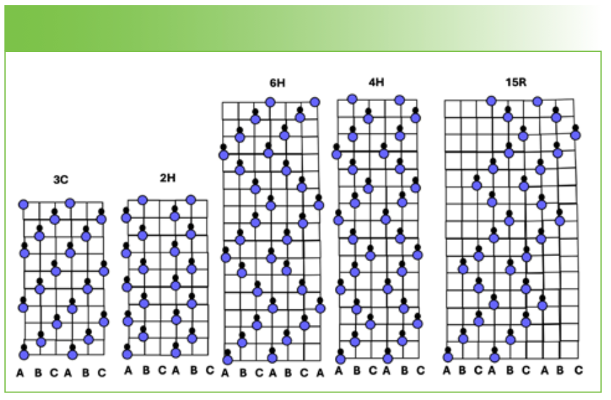
There are numerous recent publications that discuss the types of defects in silicon carbide (SiC) and how they can be analyzed. Several in my library include a discussion of Raman spectroscopy and mapping (1–3). Actually, the information in the Raman spectra of SiC polymorphs goes back to the 1960s (4,5)! To understand the structure of the various phases, it is useful to look at the cubic unit cell with one of the (111) planes depicted. Figure 1 shows the crystal structure of the cubic phase on the left (this figure shows four unit cells in the cube), and on the right, one of the (111) planes of a cube. What is interesting about this material is that the SiC bilayers lie in planes parallel to the cube’s (111) planes, and because of the (111) planes’ threefold symmetry, successive planes can be rotated by 60, 120, or 180o, all while maintaining the same nearest neighbors (6) and near-equivalent interactions between the layers (the small differences are due to the relative positioning of subsequent layers). The succession of rotations and the number of planes in the repeat unit will determine what the structure of the new phase is. Figure 2 shows the structure of some of the more common phases, and is derived from Figure 2 in (6).
FIGURE 1: (a) Crystal structure of cubic SiC; and (b) a cube with a (111) plane drawn.
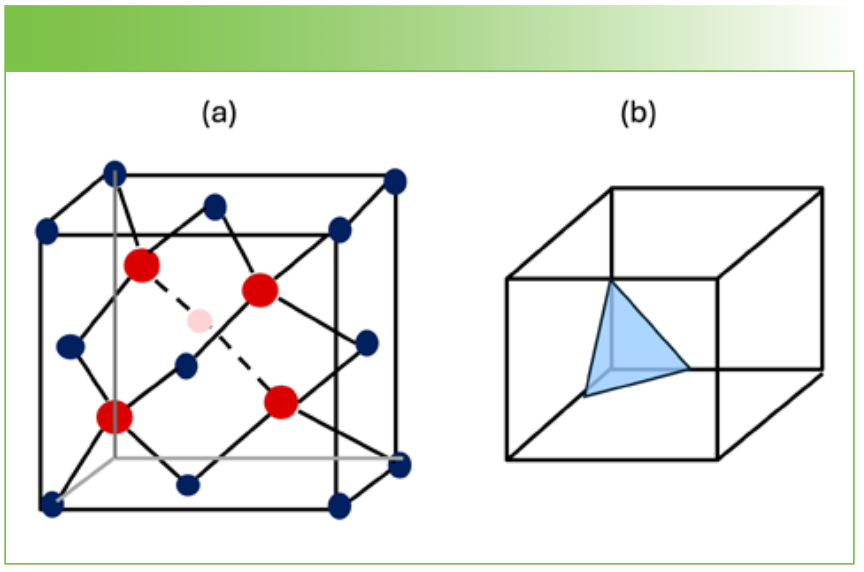
FIGURE 2: The vertical direction in these figures is the dimension where the planes are stacked. This is a (111) direction for the cubic 3C phase. Here it is clear how the planes are stacked and how they repeat. Open blue circles are Si atoms, and closed circles are carbon atoms. Figure provided by the author based on reference (6).
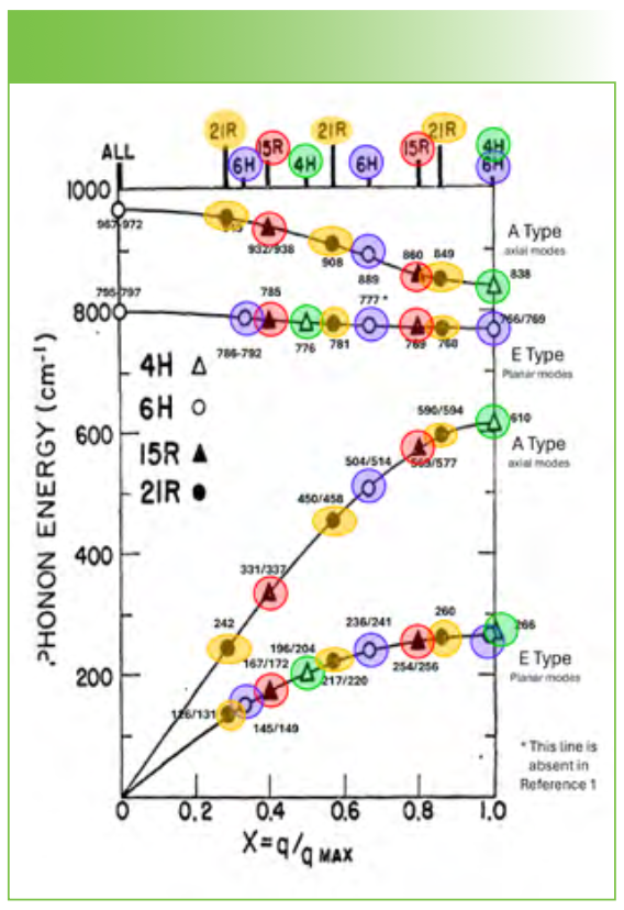
The Raman behavior of a number of SiC phases was originally measured by a group at Westinghouse Labs outside of Pittsburgh under the direction of D. W. Feldman in the late 1960s. They understood that the phonon behavior can be understood by describing the polymorphs as super-lattices—that is, each polymorph is constructed by stacking bilayers of SiC along a (111) direction, and the number and type of formula units that are stacked in a new repetition unit will determine the new phase. The new unit cells can be either hexagonal (H) type or rhombohedral (R) type with, respectively, n or 3n formula units in the unit cell. The number of formula units determines what values of the cubic phonon wavevector will allow q = 0 scattering in each new phase. By measuring the spectrum of each phase, it was possible to assign values for the dispersion behavior of the cubic phase (1,5). This is shown in Figure 3. The figure is adapted from Figure 7 in (5), but uses the phonon energies of (1) (a much more recent publication) when there were differences greater than 1 cm-1 , or when there were differences in the number of phonons in a given phase. Analysis shows that the four branches shown in the figure either have A-type or E-type symmetry, which can be confirmed with polarization measurements. Because of crystal anisotropy, phonon character and energy will be dependent on the orientation of the scattering vector, implying that the measured frequency will depend on the crystal orientation in the experimental setup so measured values may deviate a bit from the ones in Figure 3. In addition, the measured frequency can depend on strain (1), doping (1,7), and phonon confinement (8). The effects of doping have been well documented in (1), but a discussion is beyond the scope of this short article. It is important, however, to recognize that Nakashima and associates have documented the ability to measure the free carrier density in the low doping regime, a capability that will be important in characterizing industrial materials (1,7). Interested readers are encouraged to look at these references. So, in using Raman measurements to understand the origin of a defect, it is important to consider the many reasons for the spectral changes, much of which is covered in the cited references.
FIGURE 3: Phonon frequencies for the cubic phase (x = 0 only) and four other phases of SiC (4H, 6H, 15R, and 21R) when the scattering wavevector is along the Z (0001) direction. This figure is derived from Figure 7 in reference (5), but uses some phonon frequencies from reference (1).
Types of Defects
There are many types of defects that have been characterized as a basal plane dislocation (BPD), stacking fault (SF), threading edge dislocation (TED), threading screw dislocation (TSD), anti-phase domain (APD), or a micropipe hollow threading (MHT) dislocation. There can also be point defects (either a vacancy or interstitial atom) which can grow along (0001) directions. Defects can be fractions of a micron up to tens of microns in size, and are considered of special interest because they can cause high-voltage failures. There can be polytype inclusions (2) that can be analyzed, as discussed above. Micropipes (3) have been studied extensively, and can be exposed for microscopic examination by exposure to potassium hydroxide (KOH) vapors that actually enlarge the micropipes.
Work Done
The measurements that will be shown were done on samples of SiC kindly supplied by Chengye Dong from the Materials Research Institute at Penn State University. The samples were available from their projects, but our interest was in determining what type of information could be gathered from defect measurements. Defects were identified by examining the samples in dark field microscopy; the ones examined all had a similar appearance—a bright round or oval spot at the surface, and then a four-leaf clover when defocusing.
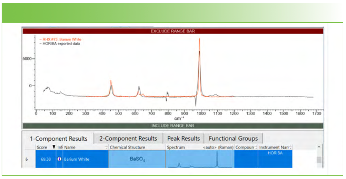
The first example that we will show is that of a foreign crystal on the surface that created what appears to be a micropipe. Figure 4 shows a spectrum of the defect (bottom) compared to a spectrum of the bulk (middle), and then the difference between the two. Classical least squares (CLS) were used to create the map on the left using the bulk spectrum (green) and the contaminant spectrum (blue). The micrographs on the right were recorded 1.5 µm above the surface, at the surface, and then 1.5 µm below the surface. Figure 5 shows the CLS map 1 µm above the surface and at 2.8 µm below the surface. The images are somewhat offset in the Y direction, which can be used to determine the orientation of the face since these micropipes are believed to follow the crystallographic growth direction. If we use the LabSpec software to scan the map from the lowest to highest Z, we find that the inclusion appears to have a diameter near 1 µm at the bottom and almost 3 µm at the top. This is consistent with a conical-shaped inclusion embedded in the SiC chip, which is the shape of a micropipe. In fact, beautiful micropipe images are seen only after etching with KOH which also enlarges the micropipe (3). Raman mapping thus provides a non-destructive method for identifying micropipes. But what is the origin of this defect? On the top of Figure 4 is a high-quality spectrum that is a result of stripping the contribution of the bulk from the defect spectrum. Figure 6 shows the result of a KnowItAll search in which BaSO4 was identified. Since I have no information on the history of these samples, I cannot comment on the origin of this unexpected contaminant, except to say that it had to be present somewhere in the preparation equipment. In addition, I want to point out that the BaSO4 was not the first hit. The compounds that appeared higher up did have the SO4+2 band near 1000 cm-1, but the other bands did not come close to matching as well as the match, as seen in Figure 6.
FIGURE 4: (a) Difference between the bottom and middle spectra; (b) Bulk spectrum; left (blue) is an image of the defect; (c) Spectrum of defect whose micrograph recorded at several depths, as shown in the righthand images.
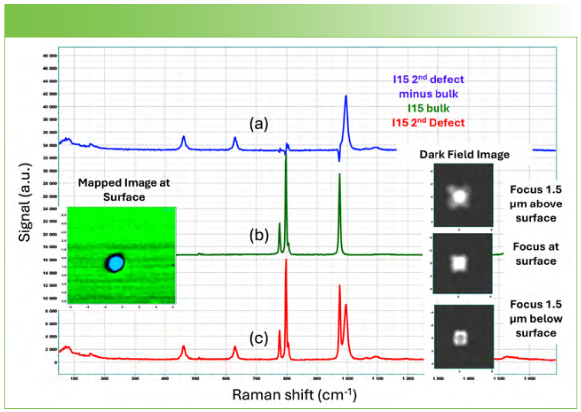
FIGURE 5: (a) Map of the defect when the microscope was imaged close to the surface vs. (b) the defect when the focus was almost 3 μm below the surface.
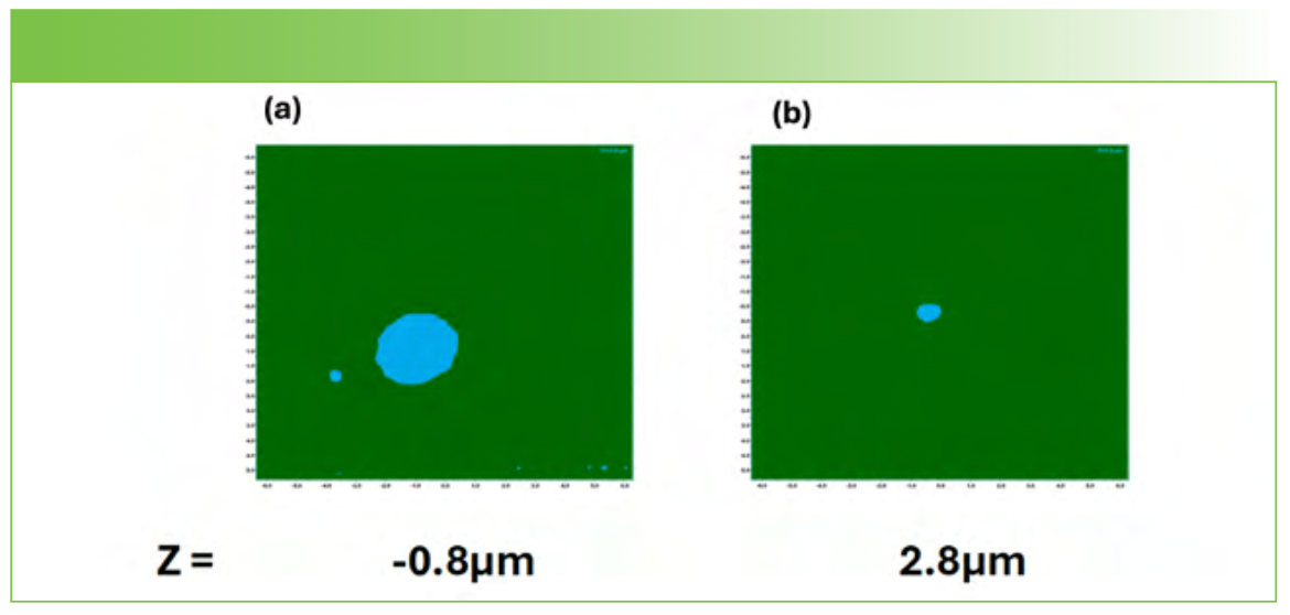
FIGURE 6: Screen capture from KnowItAll software that shows a clear indication for BaSO4 being the origin of the contaminant.
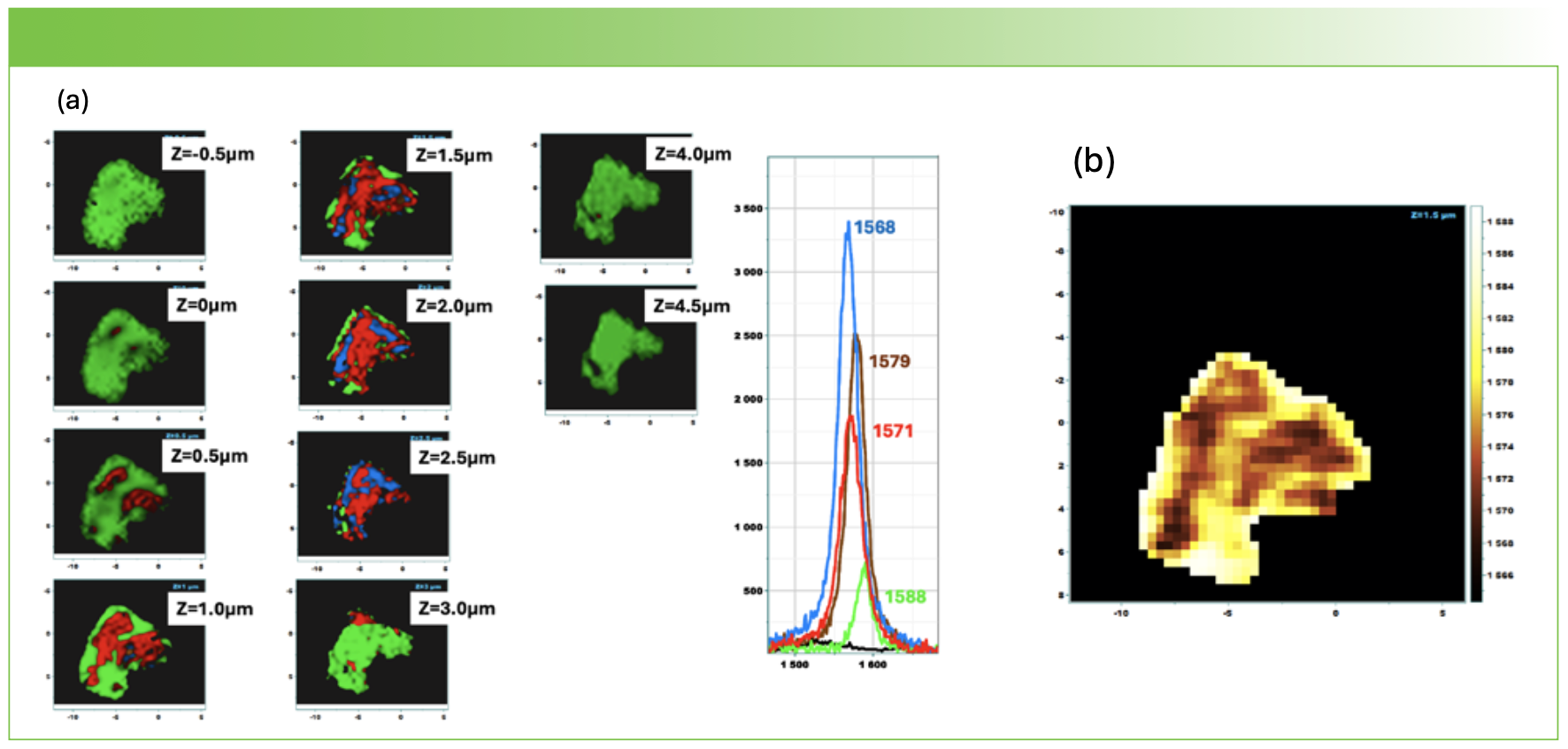
The second example that I will be showing is an instance where graphitic material appears on the surface close to one of the clover leaf defects that we found. This is actually of interest, because methods for growing graphene on (0001) surfaces of SiC are under development (9). As I surfed the hyperspectral cube, I noticed that the G band was shifting significantly, so I captured four unique spectra and used them to create CLS maps that are displayed in Figure 7a and show Raman images of different forms of graphitic material as a function of depth. Figure 7b shows the result of peak fitting the spectra to the graphite band and plotting the peak shift. In this map, the lightest color represents the highest frequency. If you compare to the 1.5 µm map in Figure 7a, you can see that the green represents the highest frequency component that was plotted, and its positions are correlated with the lightest color in the map in Figure 7b.
FIGURE 7: (a) CLS maps of four graphite spectra as a function of depth under the surface; (b) Peak fit of the same spectra shown in (a), which is a map at 1.5 μm below the surface. X- and Y-axes are spatial dimensions; Z-axis is Raman shift.
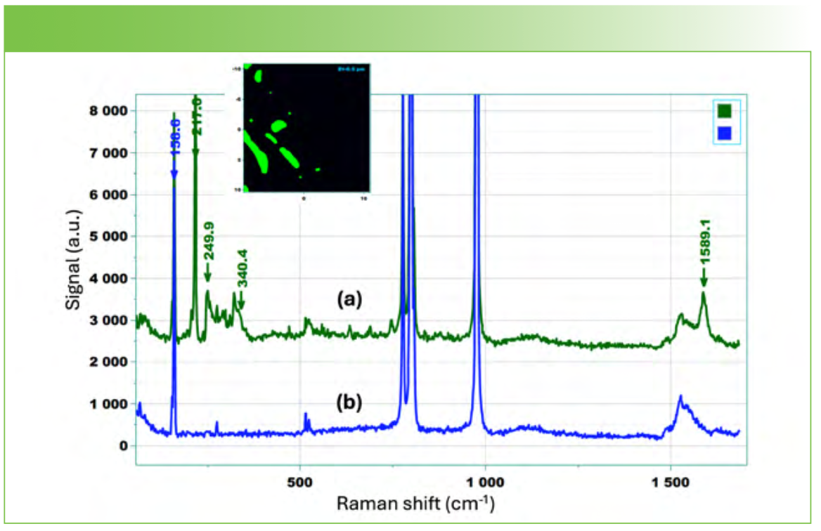
As a last example, in a data file of one of the samples, we found an “extra” sharp band at 217 cm-1. Figure 8 shows a map of this band at Z = 0.5 µm, and that of an unusual spectrum in this map where the band at 217 cm-1 occurs. Note that the band at 217 cm-1 appears at the same time that a G graphitic band appears at 1586 cm-1. Possibly of equal importance, however, is the region between 250 and 340 cm-1, where there are several bands that overlap. The systematic presence of the extra band at 217 cm-1 is suggestive of a contribution from 4H or 21R, but the presence of the overlapping features between 250 and 340 cm-1 can be attributed to defects in the stacking order of the SiC bilayers in these regions. (Refer to Figure 5 on page 50 of [1]).
FIGURE 8: (a) Map showing regions with the “extra” band at 217 cm-1 and the G graphtic band at 1589 cm-1, with corresponding image; (b) Bulk spectrum on the bottom.
Summary
In this article, I tried to provide an introduction to the structural properties of the SiC’s as revealed in their Raman spectra. With the goal of understanding how Raman microscopy can be useful in the analysis of industrial products, I described the origins of several defects that I found in these samples. I had hoped to find a defect with a clear indication of a transformation from the native 6H polymorph to a different polymorph, but the closest that I came was the last example, which indicates disorder in the stacking of the bilayers of SiC. However, I did find a surprising contaminant in one defect whose structure is suggestive of a micropipe that can be identified with KOH etching, but in this case, we did not have to destroy the sample to reveal the micropipe. In the one other treated example, I showed the distribution of different graphitic species in a graphitic layer. I tried to explain enough about the structure of this unusual class of materials, so that if any of my readers want to use Raman microscopy to analyze SiC, the basic ideas will have been introduced (with literature references), and you will be able to start your analysis. Good luck!
Acknowledgments
I want to express my appreciation to my colleague, Peng Miao, a new member of our application team. He came to us with experience measuring SiC, and provided me insights in this investigation. I also want to thank Max Werthington at Penn State who arranged to get me these samples from Chengye Dong, and provided some useful comments on this manuscript before it was submitted.
References
(1) Nakashima, S.; Harima, H. Raman Investigation of SiC Polytypes. Phys. Stat. Sol. (a) 1997, 162, 39–64. DOI: 10.1002/1521-396X(199707)162:1<39::AID-PSSA39>3.0.CO;2-L
(2) Chen, P. C..; Miao, W. C.; Ahmed, T. et al. Defect Inspection Techniques in SiC. Nanoscale Res. Lett. 2022, 17, 30. DOI: 10.1186/s11671-022-03672-w
(3) Wang, H.; Yu, J,; Hu, G.; Peng, Y.; Xie, X.; Hu, X.; Chen, X.; Xu, X. Micropipes in SiC Single Crystal Observed by Molten KOH Etching. Materials 2021, 14 (19), 5890. DOI: 10.3390/ma14195890
(4) Feldman, D. W.; Parker, Jr. J. H.; Choyke, W. J.; Patrick, L. Raman Scattering in 6H SiC. Phys. Rev. 1968, 170 (3), 698–704. DOI: 10.1103/PhysRev.170.698
(5) Feldman, D. W.; Parker, Jr. J. H.; Choyke, W. J.; Patrick, L. Phonon Dispersion Curves by Raman Scattering in SiC, Polytypes 3C, 4H, 6H, 15R, and 21R. Phys. Rev. 1968, 173 (3), 787–793. DOI: 10.1103/PhysRev.173.787
(6) van Haeringen, W.; Bobbert, P. A.; Backes, W. H. On the Band Gap Variation in SiC Polytypes. Physica Status Solidi B 1997, 202 (1), 63–79. DOI: 10.1002/1521-3951(199707)202:1<63::AID-PSSB63>3.0.CO;2-E
(7) Nakashima, S.; Kitamura, T.; Kato, T.; Kojima, K.; Kosugi, R.; Okumura, H.; Tsuchida, H.; Ito, M. Determination of Free Carrier Density in the Low Doping Regime of 4H-Si C by Raman Scattering, Appl. Phys. Let. 2008, 93, 121913. DOI: 10.1063/1.2992063
(8) Havel, M.; Baron, D.; Mazerolles, L.; Colomban, P. Phonon Confinement in SiC Nanocrystals: Comparison of the Size Determination Using Transmission Electron Microscopy and Raman Spectroscopy. Appl. Spectrosc. 2007, 61 (8), 855–859. DOI: 10.1366/000370207781540187
(9) Norimatsu, W.; Kusunoki ,M. Epitaxial Graphene on SiC{0001}: Advances and Perspectives. Phys. Chem. Chem. Phys. 2014, 16 (8), 3501–3511. DOI: 10.1039/c3cp54523g
Fran Adar is the Principal Raman Applications Scientist for Horiba Scientific in Edison, New Jersey. Direct correspondence to: SpectroscopyEdit@mmhgroup.com. ●


AI-Powered SERS Spectroscopy Breakthrough Boosts Safety of Medicinal Food Products
April 16th 2025A new deep learning-enhanced spectroscopic platform—SERSome—developed by researchers in China and Finland, identifies medicinal and edible homologs (MEHs) with 98% accuracy. This innovation could revolutionize safety and quality control in the growing MEH market.
New Raman Spectroscopy Method Enhances Real-Time Monitoring Across Fermentation Processes
April 15th 2025Researchers at Delft University of Technology have developed a novel method using single compound spectra to enhance the transferability and accuracy of Raman spectroscopy models for real-time fermentation monitoring.
Nanometer-Scale Studies Using Tip Enhanced Raman Spectroscopy
February 8th 2013Volker Deckert, the winner of the 2013 Charles Mann Award, is advancing the use of tip enhanced Raman spectroscopy (TERS) to push the lateral resolution of vibrational spectroscopy well below the Abbe limit, to achieve single-molecule sensitivity. Because the tip can be moved with sub-nanometer precision, structural information with unmatched spatial resolution can be achieved without the need of specific labels.