Stress, Strain, and Raman Spectroscopy
Stress and strain are terms that are often used interchangeably when discussing the characteristics of materials. Nevertheless, their meanings are different. Stress is a force per unit area applied to an object, and strain is the effect on the object from the stress. Specifically, strain is the change in the positions of the atoms or the lengths of the chemical bonds within the object that are induced by the application of stress. Here, we discuss the distinction of these terms, and their mathematical forms as applied to crystals. Strain is manifest in Raman spectra through changes in peak position and bandwidth. We present examples of the identification of strain in crystals of several technologically important materials.
Readers of Spectroscopy have often read how stress or strain can be detected by Raman spectroscopy through the shifting or broadening of certain bands. In this installment of "Molecular Spectroscopy Workbench," we delve more deeply into this topic, discussing the physics and mathematics of stress and strain, and demonstrating their effects on Raman spectra. We begin by carefully defining these two terms, and making the proper distinction between them. Readers interested in a deeper mathematical explanation of stress and strain are encouraged to read the two chapters on these subjects in the classic work by Nye (1).
When external forces are applied to an object that does not move, we say that it is under stress. Furthermore, if the forces on the object do not vary spatially, then the object is subject to homogeneous stress. Stress normally occurs over an area of an object, and not just a point location. Therefore, stress is properly understood as the force per unit area applied to an object, and is described mathematically by the second rank tensor shown in equation 1, where σ represents stress:

We may consider an ideal object such as a cube with the usual x, y, and z axes to better understand the components of the stress tensor. The stress forces applied along the cube's x, y, or z-axis are said to be the normal components of stress, and are associated with the tensor elements σxx, σyy, and σzz, respectively. These normal component forces can be applied inward, directed towards the center of the object, or outward. The former is defined as a compressive stress, whereas the latter is a tensile stress. The sign convention that has been adopted is that a positive value of σxx, σyy, or σzz corresponds to a tensile stress, whereas a negative value indicates a compressive stress. Now, it is important to understand and appreciate that the stress forces applied to opposite faces of our ideal cube must be of equal magnitude, but from opposite directions, for our cube to not move. That is why we can describe stress as a static force. The magnitudes of the stress forces need not be the same on the x, y, or z faces, but they must be the same on the opposite pair of faces.
The diagonal tensor elements σxx, σyy, and σzz are the normal components of stress, whereas all of the other off-diagonal tensor elements such as σxy, σyx, and σzy are the shear components. The shear tensor elements are paired under a condition of static equilibrium such that

For example, σxy = σyx would be shear forces perpendicular to the normal component σzz. In summary, the stress tensor diagonal elements describe the force per unit area as compressive or tensile normal components, and the off-diagonal tensor elements describe the shear unit area forces.
We have thus far discussed the stress tensor with respect to an ideal cubic object. We can now take those principles and begin to apply them to crystals of real chemical compounds or elements, and understand the strain induced in the crystal as a result of the application of the stress. It is critically important to understand how stress and strain differ. Strain is the change of the positions of the atoms, or the lengths of the chemical bonds within a crystal that are induced by the application of stress. Thus, for a cubic crystal such as silicon (Si), we can expect that a stress of a given magnitude applied along a crystallographic axis will produce the same degree of strain, whether it is applied along the x, y, or z crystallographic axis. However, for a uniaxial or biaxial crystal where all three crystallographic axes are not identical, the amount of strain induced by a given magnitude of stress will depend on the chemical bonding and forces along a particular crystal axis. Therefore, it is actually the changes in atomic positions and chemical bond lengths commensurate with strain that are detected in the Raman spectrum through the changes in peak position or band broadening.
The relationship between a homogeneous stress and homogeneous strain as a generalized form of Hooke's Law is given by

where εij is the strain tensor and sijkl is the elastic compliance constant of the crystalline material. The strain tensor is a second rank 3 x 3 tensor of the same form as the stress tensor shown in equation 1. Therefore, equation 4 consists of nine equations, each with nine components on the right hand side. For example,
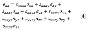
Of course, there will be eight similar equations for the remaining εxy, εxz, εyx, εyy, εyz, εzx, εzy, and εzz tensor elements. The implication of equations 3 and 4 is that, if even only one component of the stress is nonzero, σyy for example, all of the strain elements may be nonzero. Consider what that last statement could mean applied to a rectangular or even cubic crystal. If a uniaxial stress is applied to one face of the crystal, it will stretch in the direction of the applied force, but may also undergo shearing such that the angles between faces may differ from the original 90 degrees. In other words, strain may be induced in a material in a direction other than that of the applied stress.
We have discussed compressive and tensile stress, and so we can now understand the compressive and tensile strain induced in a crystal or material as a result of the application of the corresponding stress forces. If a crystal is subjected to a tensile stress, we can envision the atoms being pulled apart, or chemical bonds lengthened, relative to their normal positions and lengths in an unstressed crystal. As the chemical bond length increases, and the force constant remains the same, we should expect the vibrational frequency to decrease. A shift of the Raman peak position to lower frequencies is exactly what is observed from materials that have been subjected to a tensile stress. Conversely, if a compressive stress is applied, we would expect the atoms in a crystal to move closer together, or the chemical bond lengths to be shortened, relative to their normal positions and lengths in an unstressed crystal. The resulting compressive strain in the crystal results in Raman peak positions shifted to higher frequencies. The lesson to be learned here is that compressive and tensile stresses will induce corresponding strains in the crystal that can be observed as shifts of a Raman peak position to higher or lower frequencies, respectively. The magnitude of the Raman peak shift will be commensurate with that of the stress and corresponding strain induced in the material. The degree to which the Raman band will shift is dependent on the specific material under examination and the elastic compliance constant (sijkl) of that chemical compound or element, and the specific crystallographic axes being probed.
As you can see, the stress–strain tensor relationship in even the most simple crystal structures can be complex. Nevertheless, quantitative analysis of stress or strain by Raman spectroscopy has been performed on a variety of materials, including silicon (2–7), aluminum oxide (8–10), barium titanate (11–12), and aluminum nitride (13). Now that we have reviewed the fundamental physics of stress and strain, we can examine how they affect the Raman spectra in various technologically important materials.
Imaging Strain in Polysilicon
Much of the early work on microRaman spectroscopy of semiconductors involved the characterization of polycrystalline silicon (14–17), also known as polysilicon, which is still used extensively in fabricated electronic devices. Theoretical and experimental work was directed towards an understanding of how strain, microcrystallinity, and crystal lattice defects or disorder can all affect the Raman band shape, position, and scattering strength of single and polycrystalline silicon (18–20). The presence of nanocrystalline silicon in polysilicon was confirmed through the combination of transmission electron microscopy and Raman spectroscopy, and the effects of extremely small silicon grain dimensions on the Raman spectra were attributed to phonon confinement (21–24). As the crystalline grain size becomes smaller, comparable to the wavelength of the incident laser light or less, the Raman band broadens and shifts relative to that obtained from a crystalline domain significantly larger than the excitation wavelength. This has been explained in part by phonon confinement, in which the location of the phonon becomes more certain as the grain size becomes smaller, and therefore the energy of the phonon measured must become less certain consistent with the Heisenberg uncertainty principle.
It is important to understand the effects of nanocrystallinity on the Raman spectrum, so as not to wrongly attribute the spectral features of nanocrystals to strain in microcrystalline or larger grain sizes. Of course, strain can be present in nanocrystalline materials. If that is the case, then one will not be able to strictly differentiate the combined effects of strain and nanocrystallinity on the Raman spectrum.
A collection of data from a polysilicon test structure is shown in Figure 1. A reflected white light image of the structure appears in the lower right hand corner, and a Raman image corresponding to the central structure in the reflected light image appears to its left. The plot on the upper left consists of all of the Raman spectra acquired over the image area and the upper right hand plot is of the single spectrum associated with the cursor location in the Raman and reflected light images. The Raman data were acquired using 532 nm excitation and a 100x Olympus objective and by moving the stage in 200 nm increments over an approximate area of 25 µm × 25 µm. In this particular case, the Raman image is rendered through a color coded plot of Raman signal strength of the corresponding color bracketed Raman shift positions in the two upper traces.
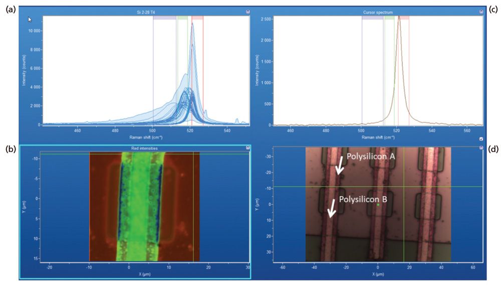
Figure 1: (a) Raman hyperspectral data set from a polysilicon test structure with (d) white reflected light image in lower right corner; (b) a Raman image generated from the spatially varying signal strengths between the color coded brackets in the spectral traces; (c) the single spectrum corresponding to the cross hairs in the Raman and white reflected light images.
Raman spectra of the unstrained substrate silicon, microcrystalline and strained polycrystalline silicon, and nanocrystalline silicon are shown in Figure 2. The substrate silicon spectrum consists of the Raman band at 521 cm-1 arising from the first order optical phonon at the Brillouin zone center. The Raman band in the spectrum of microcrystalline polysilicon appears at 515 cm-1, a shift of –6 cm-1 relative to the peak position of the unstrained substrate silicon, thereby indicating the presence of tensile strain. The increased width of the polysilicon silicon Raman band indicates that there is a distribution of strains, and the band shift is not the result of a single uniaxial stress. The shoulder at 521 cm-1 can be attributed to the substrate silicon underlying the polycrystalline silicon film. The spectrum of nanocrystalline silicon manifests substantial broadening with the peak centered at 502 cm-1. As a result, the substrate silicon signal at 521 cm-1 is now better resolved. The substantial broadening and peak center shift of approximately –19 cm-1 are consistent with phonon confinement associated with crystal grain sizes with nanometer dimensions. Of course, the nanocrystalline silicon can also be strained, but the effects of strain cannot be differentiated from those of nanocrystallinity in the Raman spectrum.
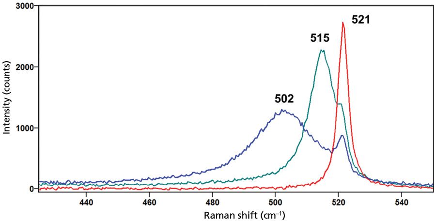
Figure 2: Raman spectra of the substrate silicon (red), microcrystalline and strained polycrystalline silicon (green), and nanocrystalline silicon (blue).
With respect to our explanation of the Raman spectra in Figure 2, we now discuss the reasoning behind our choice of the color-coded brackets to render the Raman image, and how they relate to differences in the solid-state structure of silicon. If we were to have a merely elemental compositional image of this particular structure, we would expect it to be entirely uniform without spatial variation, because silicon would appear in every pixel of the image. However, if we distinguish the different solid-state structures of the silicon by identifying unstrained silicon with the Brillouin zone center Raman band of 520.7 cm-1 isolated in red brackets, microcrystalline and strained polycrystalline silicon in green brackets, and a distribution of nanocrystallinity and strain in the blue brackets, we can render the Raman image in the lower left hand corner. To some degree strain, microcrystallinity, and nanocrystallinity are comingled in the polysilicon regions of our images; however, we can make a reasonable distinction by attributing the blue regions as primarily due to nanocrystalline grain size.
Now we consider what our rendering reveals in the Raman image, expanded for more detailed examination in Figure 3. The red regions consist of either substrate silicon or grown single crystal silicon with different oxide thicknesses. The spatial variation of the single crystal Raman signal strengths corresponds precisely with the physical optical effects of the oxide thicknesses and even small contaminants or defects seen in the reflected light image. Furthermore, because of the thinness of the polysilicon A alone, one can see through the green polysilicon A component to the underlying red substrate silicon, particularly on the left and right of the upper and lower portions of Figure 3. The spatial variation of the microcrystalline and strained polycrystalline silicon green component signal strength corresponds to both the central strip consisting of polysilicon B deposited on polysilicon A and the granular variation of polysilicon A seen in the reflected light image. Note that the polysilicon A bright green speckles in the Raman image correspond precisely to black speckles in the reflected light image. Careful examination of the central strip reveals these same speckles in the polysilicon A blurred somewhat by the polysilicon B deposited on top of it.
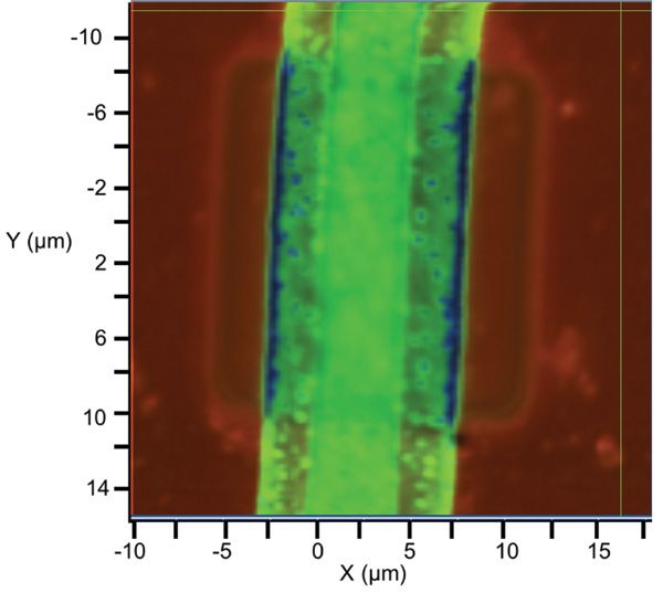
Figure 3: The Raman image from Figure 1b. Red corresponds to single crystal silicon, green to microcrystalline and strained polysilicon, and blue to nanocrystalline silicon. Polysilicon B (in the center) was deposited on the wider, underlying polysilicon A.
Now let's turn our attention to the appearance of nanocrystalline silicon in the image. The formation of nanocrystalline silicon occurs almost exclusively in polysilicon A and only on top of the central single crystal silicon structure, and not the substrate silicon. Note that the nanocrystallinity occurs primarily along the edge of the polysilicon A, but is absent as the polysilicon A continues along the silicon substrate. Also, we see that some of the polysilicon A speckles appear blue, thereby revealing nanocrystallinity over the central structure but not over the silicon substrate.
In summary, the intensity variations of the single crystal silicon comport with the physical optical effects of varying oxide film thickness and surface contaminants. Also, this Raman image reveals the spatially varying nanocrystallinity, microcrystallinity and strain in polysilicon. We can infer that these structural differences occur either as a result of processing conditions, or from interactions with the adjacent or underlying materials in which the polysilicon is in contact. The use of narrow colored brackets with our hyperspectral mapping data set allows one to differentiate strain free, strained microcrystalline, and nanocrystalline silicon and to render an image of these spatially varying solid state structures.
Strain in Diamond
The fabrication of diamond films by chemical vapor deposition (CVD) has been under development for many years now for applications including hardened surfaces, optical windows, and electrodes. The solid-state structure of these films has a direct impact on the material properties and therefore figures of merit of the final product. Crystallinity, single or poly, the number of defects, strain, and even crystal face, can affect performance. Furthermore, the uniformity of such films can affect the overall utility of the final product. Therefore, analytical methods are called for that can characterize the spatially varying structure of CVD diamond films.
To that end, we have made use of Raman polarization selection rules for the purpose of simply differentiating single from polycrystalline diamond, and to probe the extent of lattice defects, spatially varying strain, and the degree of disorder present in a crystal. We have applied polarization-orientation (P-O) Raman spectroscopy to characterize diamond films for crystallinity and strain. The reader is referred to a previous publication on P-O Raman spectroscopy to understand the theory and practical applications of this method (25).
The CVD films consisted of diamond clusters whose edge lengths ranged from approximately 5 µm to 15 µm. The faces of the diamonds are square and triangular and presumably correspond to the (100) and (111) faces, respectively. We performed P-O Raman spectroscopy on the isolated square faces for the characterization of CVD diamond crystallinity. A reflected light image of one such square face from which P-O microRaman spectra were obtained is shown in Figure 4.
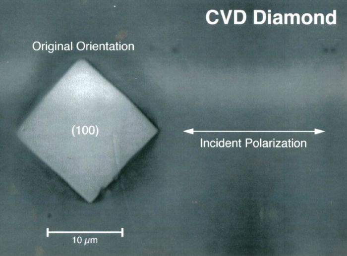
Figure 4: Reflected white light image of diamond prepared by chemical vapor deposition from which P-O microRaman spectra were obtained.
We obtained P-O Raman spectra of diamond films prepared by chemical vapor deposition using a 1.6 mW, 488.0 nm laser beam focused to a 0.6 µm diameter with an Olympus MS Plan 100 (0.95 NA) objective. Raman scattered light was collected using the same microscope objective (backscattering configuration). An analyzer was placed in front of the spectrometer entrance slit, and configured either parallel or perpendicular to the incident polarization. Individual spectra were collected at 5° rotational increments for each analyzer polarization configuration as the sample is then rotated within the focal plane. The sensitivities of the microscope and spectrometer to the two, orthogonal polarizations were characterized against a depolarized white light source. Accordingly, corrections were made to the intensities of P-O Raman spectra obtained at the corresponding polarizations.
The P-O Raman spectra shown in Figure 5 indicate that the diamond is a single crystal that contains substantial defects. The orientational dependence of the Raman spectra manifest the expected sinusoidal response for a single crystal diamond rotated in a (100) plane with the parallel and perpendicular P-O spectral plots 45° out of phase with each other. However, the failure of the signal to vanish at the minima and the presence of an amorphous carbon band at approximately 1560 cm-1 invariant with orientation reveal considerable defects in what is nominally a single crystal of diamond.
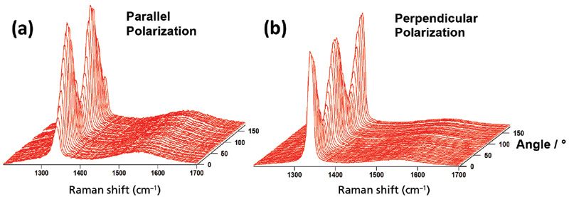
Figure 5: P-O Raman spectra of a (100) face of the CVD diamond shown in Figure 4. The light collection analyzer was oriented (a) parallel and (b) perpendicular to the incident polarization.
In addition to the defect-induced disorder manifest in the spectra, crystal orientation dependent strain can be identified through band fitting. The strain-free Raman band of diamond appears at 1333 cm-1. Previous work by other authors has demonstrated the crystallographic orientational variation of strain in diamond films and the use of polarized Raman spectroscopy to detect it (26-28). Figure 6 shows two Raman spectra from the perpendicular polarization set (Figure 5) separated by 5 rotational degrees. Band fitting reveals a strain-free component at 1333 cm-1, and a second component at 1341 cm-1, thereby indicating the presence of compressive strain. Note that the relative contributions of the strain-free to strained components of the diamond Raman band are inverted, even though the crystal has been rotated by only 5°. Indeed, the 3D variation of the strain in this crystal contributes significantly to the deviation of the experimentally obtained P-O diagram from one calculated for an ideal crystal. Were the diamond to be free of defects and spatially varying strain, we would expect the Raman signal strengths to be zero at the minima in the P-O plots shown in Figure 5.
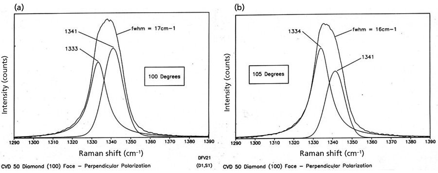
Figure 6: P-O Raman spectra separated by 5 rotational degrees for (a) versus (b). The spectra are fitted for strain-free diamond (~1333 cm-1) and a strain component.
Strain in Two-Dimensional Molybdenum Disulfide
There is a great need for characterization of two-dimensional (2D) transition metal dichalcogenide crystals because of their experimental nature and structural variability, often within one film. We have discussed the resonance Raman and photoluminescence spectroscopy and imaging of few-layer molybdenum disulfide previously (29). The spatial variation of the number of atomic layers of 2D crystals can often be inferred from the hue or color of the crystal when viewed using reflected white light microscopy, and so there have been developments to use optical microscopy to rapidly identify the number of stoichiometric layers that make up the 2D crystal (30). However, spatially varying strain in 2D crystals does not manifest itself in reflected white light images. In this article, we focus on spatially varying strain in exfoliated and chemical vapor deposition molybdenum disulfide revealed by Raman spectroscopy.
Several spectra and a Raman image of a large exfoliated molybdenum disulfide few-layer flake, and a smaller flake nearby, are shown in Figure 7. The Raman data were acquired using 532 nm excitation and a 100x Olympus objective and by moving the stage in 300 nm increments. The Raman image is a rendering of signal strength for a particular Raman band as a function of position on the sample. In this case, the Raman image is rendered through red corresponding to the Raman band of substrate silicon at 521 cm-1, and green is associated with the Raman signal of the molybdenum disulfide A1g band at 408 cm-1.
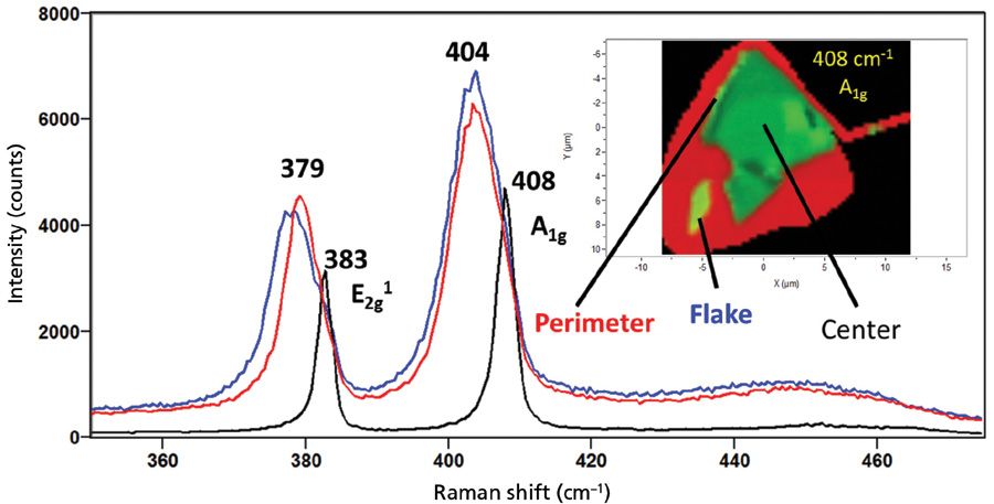
Figure 7: Raman spectra of few-layer molybdendum disulfide from different locations on the two flakes shown in the inset Raman image. The spectrum from the center is not strained. Note the substantial shifts and broadening corresponding to strain in the perimeter and flake spectra.
Most of the large flake is strain free; however, substantial tensile strain is present along a portion of the perimeter. Raman spectroscopy is most useful for identifying spatially varying and heterogeneous strain through the broadening and shifting of bands relative to those from areas free of strain. Here, the broadening and the shifting to lower wavenumber by 4 cm-1 of the E12g and A1g bands indicate the presence of tensile strain in the small flake and at the perimeter of the large flake. An interesting observation is that, very often, the structure of the perimeter of a few-layer molybdenum disulfide flake is quite different from that of the interior manifesting differences in both Raman scattering and photoluminescence.
Strain is frequently observed at the perimeters of exfoliated molybdenum disulfide few-layer flakes. It can also be detected at the perimeters and interfaces of 2D crystals grown by chemical vapor deposition. A collection of hyperspectral data and the corresponding Raman image from primarily single-layer molybdenum disulfide crystals grown on a silicon substrate are shown in Figure 8. The Raman data were acquired using 532 nm excitation and a 50x Olympus objective and by moving the stage in 1 µm increments over an area of approximately 120 µm × 90 µm. The spectra consist primarily of the E12g (382 cm-1) and A1g (402 cm-1) molybdenum disulfide bands, and the first order optical phonon from silicon at 521 cm-1. A reflected white light image of the sample area appears in the lower right hand corner, and a Raman image corresponding to the reflected light image appears to its left. The large triangular features in the white light image are single-layer molybdenum disulfide crystals, and the surrounding lighter area is the silicon substrate. The small dark area at the center of the upper triangle is two-layer molybdenum disulfide. The plot on the upper left consists of all of the Raman spectra acquired over the image area. The upper right hand plot is of the single spectrum associated with the cross hair location in the Raman and reflected light images; the line cursor is positioned at the E12g peak of strain-free molybdenum disulfide to reveal the strain at the cross hair location. The presence of shear E22g (21.2 cm-1) and inter-layer breathing B22g (37.5 cm-1) bands in the hyperspectral data set (upper left of Figure 8) from the small dark area confirms that it is two-layer molybdenum disulfide (31). These low frequency bands are absent in the spectra of single-layer molybdenum disulfide.
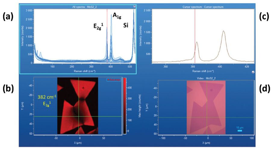
Figure 8: (a) Raman hyperspectral data set from molybdendum disulfide grown on silicon with (d) white reflected light image in lower right corner. (b) Raman image generated from the spatially varying signal strengths between the red brackets in the hyperspectral plot. (c) The single spectrum corresponding to the cross hairs in the Raman and white reflected light images; the line cursor is positioned at the E12g peak of strain-free MoS2.
The red Raman image in the lower left of Figure 8 corresponds to the E12g (382 cm-1) molybdenum disulfide band between the red brackets seen in the plot in the upper left. The Raman image is a rendering of signal strength between the brackets as a function of position on the sample. In this particular case, the red brackets have been made narrow, and placed around the E12g (382 cm-1) band as it appears in the interior of the crystal away from both the perimeter and crystal interfaces. Narrowing the brackets allows them to function as a spectral slit in the image generation; Raman bands that shift to lower or higher frequency will manifest decreased intensity as less of the band will appear between the narrow brackets. Consequently, areas of strain will show diminished signal strength and appear darker in the Raman image, because the Raman band has shifted to either lower or higher frequency depending on whether the strain is tensile or compressive, respectively.
We need to carefully examine the spectra from the Raman map in Figure 8 to understand how the narrow brackets function as a spectral slit to reveal strain and even the two-layer molybdenum disulfide in the Raman image. Representative spectra of the interior single-layer molybdenum disulfide, perimeter, strained crystal interface, and dark two-layer molybdenum disulfide are shown in Figure 9. The Raman spectrum of the interior single-layer molybdenum disulfide free of strain consists of the E12g (381.6 cm-1) and A1g (402.1 cm-1) bands. The Raman spectrum of the dark two-layer molybdenum disulfide consists of the E12g (379.9 cm-1) and A1g (403.3 cm-1) bands having peak positions -1.7 cm-1 and +1.2 cm-1, respectively, relative to those of the single-layer molybdenum disulfide. The increased separation of the E12g and A1g bands, along with the aforementioned presence of the low frequency bands, confirms that the small dark area in the upper triangle is two-layer molybdenum disulfide. The E12g (381.4 cm-1) and A1g (401.4 cm-1) bands in the spectrum of the perimeter have shifted to -0.2 cm-1 and -0.7 cm-1, respectively, thereby indicating the presence of a tensile strain at the perimeter. The E12g (382.9 cm-1) and A1g (402.7 cm-1) bands in the spectrum of the strained crystal interface (the dark areas between the crystals) have shifted to +1.3 cm-1 and +0.6 cm-1, respectively, thereby indicating the presence of a compressive strain. The E12g band shift is twice that of the A1g band and so the selection to bracket the E12g band makes it a better choice for revealing spatially varying strain at the crystal interfaces in the Raman image.
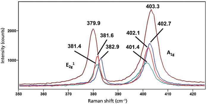
Figure 9: Raman spectra obtained from different locations of sample shown in Figure 8: Interior single-layer molybdendum disulfide (red), perimeter (green), strained crystal interface (blue), and dark two-layer molybdendum disulfide (brown).
Now we consider what our rendering reveals in the Raman image expanded for more detailed examination in Figure 10. We choose a single spectral component color image with spectrally narrow brackets to reveal the spatially varying strain associated with the chosen Raman band. In this particular case, the red brackets have been made narrow, and placed around the E12g (382 cm-1) band as it appears in the interior of the crystal away from both the perimeter and crystal interface. Using a narrow bracket allows it to function as a spectral slit in the image generation, thereby differentiating the strain-free single-layer molybdenum disulfide from the strained areas, as well as the two-layer molybdenum disulfide. As explained above, areas of strain appear darker in the Raman image because the band has shifted and contributes less signal strength within the narrow spectral brackets. The spectra in Figure 9 revealed the compressive strain at the interfaces of the triangular molybdenum disulfide crystals where the E12g band has shifted by as much as +1.3 cm-1. Consequently, the Raman image of the adjoining single-layer molybdenum disulfide crystals appears darkest precisely at the interfaces where the crystals met upon their individual growth. Note that the darkness at the interfaces projects diffusely for micrometers into the crystal, thereby revealing the projection of spatially varying and diminishing strain at some distance from the interface into the interior of the crystal. Of course, the spatially varying strain seen in the Raman image is not detected in the reflected white light image. Raman imaging has revealed a distribution of strain in the crystals that could not have been known based upon the appearance of the reflected white light image.
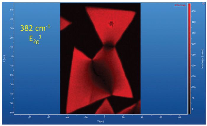
Figure 10: The Raman image from Figure 8b. Red corresponds to the narrow bracketed E2g2 band centered at 381.6 cm-1. The interfacial areas appear dark because the E2g2 band has shifted to higher wavenumber due to compressive stress.
Another collection of hyperspectral data and the corresponding Raman image of single-layer, two-layer and three-layer molybdenum disulfide crystals grown on a silicon substrate are shown in Figure 11. The triangle in the center of the reflected white light image (lower right) consists of spatially varying two-layer, and three-layer molybdenum disulfide, the pink circle surrounding the triangle is single-layer molybdenum disulfide, and the area outside of the circle is the bare silicon substrate. The red Raman image in the lower left of Figure 11 corresponds to the spatially varying signal strength of the E12g (382 cm-1) molybdenum disulfide band between the red brackets seen in the spectral plots. The plot on the upper right is of the single spectrum associated with the cross hair location at the interface of the multilayer triangle and single-layer molybdenum disulfide; note the splitting of the A1g band.
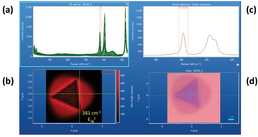
Figure 11: (a) Raman hyperspectral data set from molybdendum disulfide grown on silicon with (d) white reflected light image in lower right corner. The Raman image (b) was generated from the spatially varying signal strengths between the red brackets in the spectral plots. (c) The single spectrum corresponds to the cross hairs in the Raman and white reflected light images.
We examine the spectra from the Raman map in Figure 11 to understand the basis for the contrast between the single-layer molybdenum disulfide and the spatially varying two- and three-layer molybdenum disulfide triangle and the bright interface around the multilayer molybdenum disulfide triangle in the Raman image. Representative spectra of the single-layer molybdenum disulfide, triangle and single-layer molybdenum disulfide interface, and three-layer molybdenum disulfide are shown in Figure 12. The Raman spectrum of the single-layer molybdenum disulfide free of strain consists of the E12g (382.1 cm-1) and A1g (402.3 cm-1) bands. The Raman spectrum of the triangular three-layer molybdenum disulfide consists of the E12g (378.2 cm-1) and A1g (404.1 cm-1) bands having peak positions –3.9 cm-1 and +1.8 cm-1, respectively, relative to those of the single-layer molybdenum disulfide. The increased separation of the E12g and A1g (–3.9 cm-1 and +1.8 cm-1) bands relative to the separation of the two-layer molybdenum disulfide in Figure 9 (–1.7 cm-1 and +1.2 cm-1) confirms that the area of the triangle from which this spectrum was generated is three-layer molybdenum disulfide. Further support for this interpretation is how much broader the E12g and A1g bands in the spectrum of three-layer molybdenum disulfide are relative to their counterparts in the two-layer molybdenum disulfide spectrum. The shift of the E12g band to lower wavenumber away from the narrow brackets centered at 382.1 cm-1 is the basis for the diminished signal strength and dark appearance of the spatially varying two-layer and three-layer molybdenum disulfide triangle.
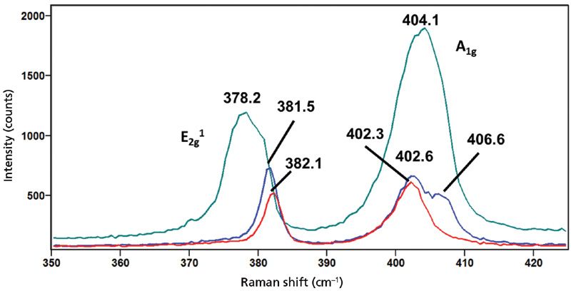
Figure 12: Raman spectra obtained from different locations of sample shown in Figure 11: Surrounding single-layer molybdendum disulfide (red), triangle and single-layer molybdendum disulfide interface (blue), and three-layer molybdendum disulfide (green).
The interface of the spatially varying two-layer and three-layer molybdenum disulfide triangle adjoining the single layer molybdenum disulfide presents a structurally different case from the crystal interface of the single-layer molybdenum disulfide crystals that have grown to meet each other. Here, we see a splitting of the A1g band. The E12g (381.5 cm-1) and A1g (402.6 and 406.6 cm-1) bands in the spectrum of the triangle and single-layer molybdenum disulfide interface have shifted to –0.6 cm-1 and (+0.3 cm-1 and +4.3 cm-1) which is very different from either the perimeter or strained crystal interface spectra in Figure 9. The spectral interpretation at this interface is not as straightforward, because of the convolution of the multilayer and single layer molybdenum disulfide signals within the same spectrum. We may interpret the E12g (381.5 cm-1) and A1g (402.6 cm-1) bands at the crystalline interface as consistent with a transition from the single-layer to two-layer molybdenum disulfide. However, the second A1g (406.6 cm-1) band is substantially shifted, +4.3 cm-1, relative to the single-layer molybdenum disulfide A1g (402.3 cm-1) band, thereby indicating a compressive strain at the interface.
The symmetry species and the directions of the atomic motions of the phonon modes affected by stress can help us to understand the differences observed in the images and spectra of Figures 8–12. The E12g band arises from in plane (xy-axes) atomic motions whereas the A1g band is associated with vibrations along the z-axis (31). Therefore, these bands will be sensitive to strain in orthogonal directions in the crystal, the doubly degenerate E12g band in the xy-plane and the A1g band along the z-axis (32–33). The large shift of +4.3 cm-1 for the second A1g band in the spectrum of the triangle multilayer–single-layer molybdenum disulfide interface is indicative of a significant compressive strain along the z-axis, whereas there is no indication of strain in the xy-plane based upon the peak position of the E12g band. This is quite different from the interfaces created by the growth of single-layer molybdenum disulfide crystals meeting each other. In the case of the contiguous single-layer molybdenum disulfide crystals, the E12g and A1g bands in the spectrum of the strained crystal interface (the dark area between the crystals) have shifted by as much as +1.3 cm-1 and +0.6 cm-1, respectively, thereby indicating the presence of a compressive strain in the xy-plane and along the z axis. In contrast, a compressive strain of far greater magnitude appears only along the z-axis at the triangle multilayer–single-layer molybdenum disulfide interface.
Conclusion
Stress and strain were defined, and a mathematical description of their relationship was provided, making the proper distinction between the two terms. Stress is a force per unit area applied to an object, and strain is the effect on the object from the stress. Specifically, strain is the change in the positions of the atoms, or the lengths of the chemical bonds within the object that are induced by the application of stress. Compressive and tensile stresses will induce corresponding strains in the crystal, which can be observed as shifts of a Raman peak position to higher or lower frequencies, respectively. The magnitude of the Raman peak shift will be commensurate with that of the stress and corresponding strain induced in the material. The degree to which the Raman band will shift is dependent upon the specific material under examination, the elastic compliance constant (sijkl) of that chemical compound or element, and the specific crystallographic axes being probed.
Raman spectroscopy is sensitive to strain, and has therefore been successfully used for the characterization of strain in materials. Raman spectra of the unstrained substrate silicon, microcrystalline and strained polycrystalline silicon, and nanocrystalline silicon from a silicon device test structure were presented and formed the basis of a Raman image. The Raman image of the test structure revealed the spatially varying nanocrystallinity, microcrystallinity and strain in polysilicon. Strain was also identified in diamond films prepared by chemical vapor deposition. We have applied polarization-orientation Raman spectroscopy to characterize diamond films for crystallinity and strain. Band fitting reveals a strain-free component at 1333 cm-1 and a second component at 1341 cm-1, thereby indicating the presence of compressive strain.
Lastly, we discussed spatially varying strain in exfoliated and chemical vapor deposition molybdenum disulfide revealed by Raman spectroscopy. Most of the exfoliated flake is strain free; however, substantial tensile strain is present along a portion of the perimeter. Raman spectroscopy is useful for identifying spatially varying and heterogeneous strain in exfoliated molybdenum disulfide through the broadening and shifting of bands relative to those from areas free of strain. Strain was also detected at the perimeters and interfaces of 2D crystals grown by chemical vapor deposition. The Raman image of adjoining single-layer molybdenum disulfide crystals revealed strain at the interfaces where the crystals met upon their individual growth. The strain projects diffusely for micrometers into the crystal. The strain is greatest at the crystal interface and spatially varies and diminishes at some distance from the interface into the interior of the crystal. Here, the E12g and A1g bands in the spectrum of the strained crystal interface have shifted by as much as +1.3 cm-1 and +0.6 cm-1, respectively, thereby indicating the presence of a compressive strain in the xy-plane and along the z-axis. The spatially varying strain seen in the Raman image is not detected in the reflected white light image. Contrast was observed in a second Raman image between the single-layer molybdenum disulfide and the spatially varying two- and three-layer molybdenum disulfide triangle and the bright interface around the multi-layer molybdenum disulfide triangle. We interpret the E12g (381.5 cm-1) and A1g (402.6 cm-1) bands at the crystalline interface as consistent with a transition from the single-layer to two-layer molybdenum disulfide. However, the second A1g (406.6 cm-1) band is substantially shifted, +4.3 cm-1, relative to the single-layer molybdenum disulfide A1g (402.3 cm-1) band, thereby indicating a compressive strain at the interface. Compressive strain appears only along the z-axis at the triangle multilayer–single-layer molybdenum disulfide interface. This is quite different from the interface created by the growth of single-layer molybdenum disulfide crystals meeting each other.
References
(1) J.F. Nye, Physical Properties of Crystals (Oxford University Press, 1985), pp. 82-109.
(2) G.H. Loechelt, N.G. Cave and J. Menendez, Appl. Phys. Lett.66, 3639–3641 (1995).
(3) G.H. Loechelt, N.G. Cave, and J. Menendez, J. Appl. Phys.86, 6164–6180 (1999).
(4) I. De Wolf, H. Norstrom, and H.E. Maes, J. Appl. Phys.74, 4490–4500 (1993).
(5) S.C. Jain, H.E. Maes, K. Pinardi, and I. De Wolf, J. Appl. Phys.79, 8145–8165 (1996).
(6) I. De Wolf, J. Raman Spectrosc.30, 877–883 (1999).
(7) T. Miyatake and G. Pezzotti, J. Appl. Phys. 110, 093511 (2011).
(8) W. Zhu and G. Pezzotti, Phys. Status Solidi A208, 1141–1150 (2011).
(9) W. Zhu and G. Pezzotti, J. Raman Spectrosc.42, 2015–2025 (2011).
(10) G. Pezzotti and W. Zhu, Phys. Chem. Chem. Phys.17, 2608–2627 (2015).
(11) G. Pezzotti, M. Higashino, K. Tsuji, and W. Zhu, J. Eur. Ceramic Soc.30, 199–204 (2010).
(12) G. Pezzotti, K. Okai and W. Zhu, J. Appl. Phys.111, 013504 (2012).
(13) W. Zhu and G. Pezzotti, Microelectron. Reliab.55, 66–73 (2015).
(14) Y. Inoue, S. Nakashima, A. Mitsuishi, T. Nishimura, and Y. Akasaka, Jpn. J. Appl. Phys.25, 798–801(1986).
(15) D. R. Tallant, T. J. Headley, J. W. Medernach, and F. Geyling, Mat. Res. Soc. Symp. Proc.324, 255–260 (1994).
(16) D. V. Murphy and S. R. J. Brueck, Mat. Res. Soc. Symp. Proc.17, 81–94 (1983).
(17) G. Harbeke, L. Krausbauer, E. F. Steigmeier, A. E. Widmer, H. F. Kappert, and G. Neugebauer, Appl. Phys. Lett.42, 249–251 (1983).
(18) G.-X. Cheng, H. Xia, K.-J. Chen, W. Zhang and X.-K. Zhang, Phys. Stat. Sol.A118, K51–K54 (1990).
(19) N. Ohtani and K. Kawamura, Solid State Commun. 75, 711–715 (1990).
(20) H. Richter, Z. P. Wang, and L. Ley, Solid State Commun.39, 625–629 (1981).
(21) Z. Iqbal and S. Veprek, SPIE Proc.794, 179–182 (1987).
(22) V. A. Volodin, M. D. Efremov, and V. A. Gritsenko, Solid State Phenom.57-58, 501–506 (1997).
(23) Y. He, C. Yin, G. Cheng, L. Wang, X. Liu, and G. Y. Hu, J. Appl. Phys.75, 797–803 (1994).
(24) H. Xia, Y. L. He, L. C. Wang, W. Zhang, X. N. Liu, X. K. Zhang, D. Feng, and H. E. Jackson, J. Appl. Phys.78, 6705–6708 (1995).
(25) D. Tuschel, Spectroscopy27(3), 22–27 (2012).
(26) S.-A. Stuart, S. Prawer, and P.S. Weiser, Diamond Related Mater.2, 753–757 (1993).
(27) T. Gries, L. Vandenbulcke, P. Simon, and A. Canizares, J. Appl. Phys.102, 083519 (2007).
(28) T. Gries, L. Vandenbulcke, P. Simon, and A. Canizares, J. Appl. Phys.104, 023524 (2008).
(29) D. Tuschel, Spectroscopy30(3) 14–29 (2015).
(30) H. Li, J. Wu, X. Huang, G. Lu, J. Yang, X. Lu, Q. Xiong, and H. Zhang, ACS Nano7, 10344–10353 (2013).
(31) X. Zhang, W.P. Han, J.B. Wu, S. Milana, Y. Lu, Q.Q. Li, A.C. Ferrari, and P.H. Tan, Phys. Rev.B87, 115413 (2013).
(32) B. Amorim, A. Cortijo, F. de Juan, A.G. Grushin, F. Guinea, A. Gutierrez-Rubio, H. Ochoa, V. Parente, R. Roldan, P. San-Jose, J. Schiefele, M. Sturla, and M.A.H. Vozmediano, Phys. Reports617, 1–54 (2016).
(33) M. Yagmurcukardes, C. Bacaksiz, E. Unsal, B. Akbali, R.T. Senger, and H. Sahin, Phys. Rev. B97, 115427 (2018).
David Tuschel

David Tuschel is a Raman applications manager at Horiba Scientific, in Edison, New Jersey, where he works with Fran Adar. David is sharing authorship of this column with Fran. He can be reached at: SpectroscopyEdit@UBM.com

AI-Powered SERS Spectroscopy Breakthrough Boosts Safety of Medicinal Food Products
April 16th 2025A new deep learning-enhanced spectroscopic platform—SERSome—developed by researchers in China and Finland, identifies medicinal and edible homologs (MEHs) with 98% accuracy. This innovation could revolutionize safety and quality control in the growing MEH market.
New Raman Spectroscopy Method Enhances Real-Time Monitoring Across Fermentation Processes
April 15th 2025Researchers at Delft University of Technology have developed a novel method using single compound spectra to enhance the transferability and accuracy of Raman spectroscopy models for real-time fermentation monitoring.
Nanometer-Scale Studies Using Tip Enhanced Raman Spectroscopy
February 8th 2013Volker Deckert, the winner of the 2013 Charles Mann Award, is advancing the use of tip enhanced Raman spectroscopy (TERS) to push the lateral resolution of vibrational spectroscopy well below the Abbe limit, to achieve single-molecule sensitivity. Because the tip can be moved with sub-nanometer precision, structural information with unmatched spatial resolution can be achieved without the need of specific labels.