Low-Dimensional WS2 Characterization with Correlative Microscopy
Application Notebook
Transition metal dichalcogenides (TMDs) display physical characteristics that hold great promise for applications in nano- and optoelectronics. These properties are strongly influenced by thickness, edge structures, lattice point defects, and functionalization of the material. For comprehensive structural and chemical characterization of low-dimensional TMDs, more than one technique is required. Here we present an analysis of WS2 flakes using correlative confocal Raman imaging and AFM.

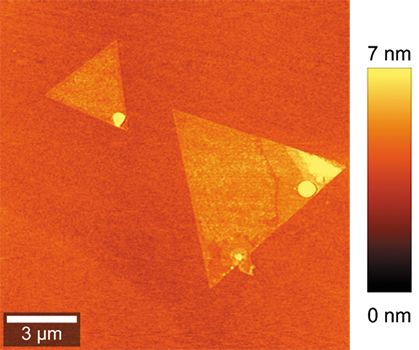
Figure 1a: High resolution AFM image of CVD-grown WS2 flakes on a Si/SiO2 substrate with varying numbers (1, 2, >2) of layers and a total height of up to 7 nm.
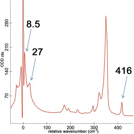
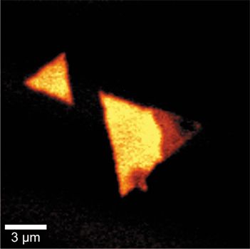
Using a confocal Raman-AFM microscope of the new WITec alpha300 microscope series, Raman spectra and the photoluminescence of CVD-grown WS2 flakes on Si/SiO2 were analyzed. AFM unambiguously revealed the numbers of atomic layers by measuring the height of the material (Figure 1a). However, this can also be determined by the material's Raman spectra with an excitation wavelength of 532 nm. Using a RayShield coupler, several peaks could be identified and were used for analysis (Figure 1b). The low frequency Raman signal at 8.5 relative wavenumbers (cm-1) assessed as being specific for single-layer (1L) structures. This band corresponded perfectly with the 1L WS2 in the AFM image and decreased with the number of layers (Figure 1c). The peak at 416 relative wavenumbers (cm-1) increased incrementally with the number of layers (not shown).

Figure 1b: Raman bands at low wavenumbers detected with RayShield technology. Excitation wavelength = 532 nm.
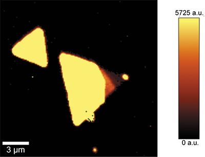
Another direct indicator of the physical and morphological features of TMDs is their photoluminescence (PL) that results from the recombination of carriers generated by photoexcitation. Its intensity and position are functions of the bandgap and thus depend on the layer count, because only the direct bandgap present in 1L WS2 allows for direct recombination of electrons and holes. Therefore PL intensity is strongest in TMD monolayers. WS2 shows strong PL around 639 nm wavelength (not shown). In the microscope image the highest PL intensity correlated perfectly with the AFM and Raman data of the monolayer flake (Figure 1d).

Figure 1c: The peak intensity map of the WS2 Raman signal at 8.5 relative wavenumbers (cm-1) corresponds well with the 1L WS2 in the AFM image. The signal decreases with the number of layers.
Conclusion
In the case of low-dimensional TMDs, photoluminescence can serve as an effective method for investigating the electronic band structure as well as the local chemical structure of the material. Uniform PL at 8.5 relative wavenumbers (cm-1) detected with WITec RayShield technology provides clear evidence of high quality 1L WS2 crystals, whereas intensity shifts indicate structural inconsistencies and local modifications. The correlation of PL data with Raman imaging and AFM yields a comprehensive picture of the material.

Figure 1d: The intensity of the PL at about 635 nm after excitation at 532 nm matches well to the thickness of the material. The fewer the layers the stronger is the PL. This can be explained by the transition of a direct bandgap in 1L WS2 to an indirect bandgap in multilayer material. The upper left 1L WS2 triangle shows strong and uniform PL.
Sample courtesy of Ting Yu, Nanyang Technological University, Singapore.
WITec GmbH
Lise-Meitner-Stra e 6, 89081 Ulm, Germany
tel. +49 (0) 731 149 700, fax +49 (0) 731 149 70 200
Website: www.witec.de
