Analyzing Solar Cell Material Properties with Confocal Raman Microscopy
Energy generation using photovoltaic devices is regarded as an important component in overcoming future energy shortages. This is reflected in a dramatic increase in photovoltaic production and demand. In the research and development of photovoltaic devices, the primary goals are to increase the conversion efficiency of the solar cells or to improve the production process. The following study describes the application of Confocal Raman Imaging for the analysis of stress fields around laser-drilled holes on a Si solar cell using the large area scanning capabilities of the WITec alpha500 Confocal Raman Microscope.
Energy generation using photovoltaic devices is regarded as an important component in overcoming future energy shortages. This is reflected in a dramatic increase in photovoltaic production and demand. In the research and development of photovoltaic devices, the primary goals are to increase the conversion efficiency of the solar cells or to improve the production process. The following study describes the application of Confocal Raman Imaging for the analysis of stress fields around laser-drilled holes on a Si solar cell using the large area scanning capabilities of the WITec alpha500 Confocal Raman Microscope.

Figure 1
Stress Fields Surrounding a Laser-Drilled Hole on a Si Solar Cell Device
In order to allow the contacts for discharging to be located on the bottom of a Si-solar cell for better efficiency, holes need to be drilled through the solar cell which is typically done with lasers. The drilling process however can induce strain in the Si around the holes, which in turn lowers the efficiency of the solar cells. In this study two ways of minimizing the stress are investigated:
1. Minimizing the laser power for drilling using
a) 100% drilling power with 9 repetitions
b) 20% drilling power with 20 repetitions
2. Etching the wafer after the drilling process:
a) no etching
b) 1 Minute with KOH
c) 2 Minutes with KOH
d) 4 Minutes with KOH
e) 6 Minutes with KOH
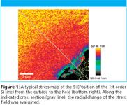
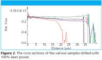
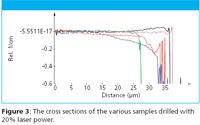
In order to evaluate the strain induced by the drilling on the Si around the holes, a WITec alpha500 Confocal Raman Imaging system with a 532nm excitation laser and a 100x air objective (NA 0.9) was used. For each image the 1st order Si peak was fitted using a Lorentzian curve and the exact peak position was then evaluated. This could also be shown as an image (Fig. 1). From these images, cross-sections as shown in Fig. 1 were extracted and plotted as relative peak positions (in rel.1/cm) vs. distance (note that the starting point relative to the edge of the hole varies for each line). Figures 2 and 3 show the results of these evaluations. Fig. 2 shows the results for the samples with full drilling power and the different etching processes applied to the samples are indicated by the colors [no etching (red), 1 min etching (blue), 2 min etching (green), 4 min etching (black), 6 min etching (magenta)]. Fig. 3 uses the same color coding, but shows the results for the cases drilled with only 20% power. For most graphs a slight decrease in the peak position can be seen starting from the left side of the graph and moving towards the position of the drilled hole. These are presumably long-range stress fields in the Si. Close to the edge of the hole, the stress in the Si increases and changes dramatically and then inside the hole, no proper Si signal could be detected.

Figure 2
From Fig. 2 it can clearly be seen that the sample which had not been etched as well as the sample which had been etched for only 1 minute show a clear drop of the peak position before reaching the edge of the hole. This drop is eliminated for the other cases. From Fig. 3 the same conclusion as above can be drawn. Additionally, the graphs seem to indicate that the soft drilling process reduces the far reaching stress field (the slope of the lines). Both graphs indicate that an etching process of 2 minutes is sufficient.

Figure 3
WITec GmbH
Hoervelsinger Weg 6 • 89081 Ulm • Germany
Tel. +49 (0) 731 14070-0

Thermo Fisher Scientists Highlight the Latest Advances in Process Monitoring with Raman Spectroscopy
April 1st 2025In this exclusive Spectroscopy interview, John Richmond and Tom Dearing of Thermo Fisher Scientific discuss the company’s Raman technology and the latest trends for process monitoring across various applications.
A Seamless Trace Elemental Analysis Prescription for Quality Pharmaceuticals
March 31st 2025Quality assurance and quality control (QA/QC) are essential in pharmaceutical manufacturing to ensure compliance with standards like United States Pharmacopoeia <232> and ICH Q3D, as well as FDA regulations. Reliable and user-friendly testing solutions help QA/QC labs deliver precise trace elemental analyses while meeting throughput demands and data security requirements.