Characterization of Amorphous and Microcrystalline Silicon Using Raman Spectroscopy
Abstract
Abstract
Silicon deposited on glass or silicon carbide is widely used in manufacturing photovoltaic cells. Both the proportion and distribution of amorphous and crystalline silicon are critical for performance and are therefore important to monitor. Raman spectroscopy is an ideal technique for this application, as the two forms generate readily distinguishable spectra that lend themselves to simple quantification methods using Beer's Law. Mapping generates chemical images with detailed information on the spatial distribution of the crystalline and amorphous forms. Since excess excitation laser power can be demonstrated to convert amorphous into crystalline silicon, care must be taken to limit the amount of power used. The Thermo Scientific DXR Raman microscope, which is equipped with a laser power regulator, is ideal for this application, particularly if the method has to be replicated from instrument to instrument at multiple manufacturing plants.
Introduction
One of the more widely used photovoltaic cell technologies employs silicon deposited on either glass or silicon carbide. Although panels were made initially with either crystalline or amorphous silicon, a judicious combination of the two materials takes advantage of the benefits of each while minimizing their respective disadvantages. Optimal performance depends on reliably being able to make cells with a predetermined ratio and distribution of the two forms. Monitoring ensures the manufacture of economical, highly efficient and long-lasting solar cells.
This is an application for which Raman spectroscopy is particularly well suited. Silicon-silicon bonds are symmetrical and result in strong Raman scattering. Crystalline silicon has highly uniform bond angles and bond lengths and exists in a limited number of states. This results in sharp Raman peaks with a characteristic strong band at 521 cm–1 . Amorphous silicon is less orderly in its arrangement with a wider array of bond angles, bond energies and bond lengths in addition to dangling bonds. The distribution of possible states leads to a broad Raman band centered at 480 cm–1 that is readily distinguishable from that of crystalline silicon.
Raman spectroscopy can be used to quantify the relative amounts of amorphous and crystalline silicon in thin layer deposits. By mapping an area of deposited silicon the uniformity of the distribution of the two silicon forms can be monitored. This application note shows typical results and discusses some of the practical aspects and potential pitfalls of using Raman spectroscopy for measuring amorphous and crystalline silicon.
Experimental
All spectra were collected using a Thermo Scientific DXR Raman microscope equipped with a 532 nm excitation laser, a full range grating and a motorized stage. The instrument was operated using the Thermo Scientific OMNIC 8 software suite. OMNIC™ Atlμs™ mapping software was used to collect and analyze mapping data.
Results
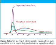
Crystalline versus amorphous silicon: Figure 1 shows typical silicon spectra from samples that range from pure crystalline to those containing significant amounts of amorphous material. The strong band at 521 cm–1 of the crystalline sample very distinct from the broad band centered at 480 cm–1 that is exhibited by the amorphous silicon. These clearly distinguishable spectra make it possible to use a simple Beer's law calculation based on the ratio of the peak heights at 521 cm–1 and 480 cm–1 to estimate the relative amounts of the two forms.

Figure 1
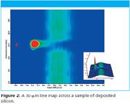
Distribution of amorphous and crystalline silicon: Raman mapping is an excellent way to obtain information about potential variations in crystallinity over areas of deposited silicon. By mounting the sample on a motorized stage and collecting Raman spectra at specified intervals across the sample, it is possible by analyzing the spectra to determine the distribution of the silicon forms. Figure 2 shows a 30-micron line map across a sample of deposited silicon. The strong Raman band at 521 cm–1 at about half way across the map shows that there is a small region of crystalline silicon at this location. The remainder of the mapped sample shows the broad Raman band at 480 cm–1 that is characteristic of amorphous material.

Figure 2
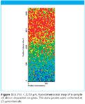
A two-dimensional (x, y) map collected across a boundary region between crystalline and amorphous forms is shown in Figure 3. In this case OMNIC Atlµs software was used to display the spectral data as a chemical image of the distribution of the two forms by calculating the ratio of the peak heights at 521 cm–1 and 480 cm–1 . The map shows the gradient between the two forms and can be used as a quality check during manufacture.

Figure 3
Considerations in Using Raman Spectroscopy for Silicon Analysis
Laser power: The results show that as the power of the excitation laser is increased above a threshold, amorphous silicon is converted to the crystalline form. The DXR Raman microscope used in these experiments features a laser power regulator which uses a feedback mechanism to control closely the amount of laser power delivered to the sample. This is important, as laser power output can vary quite markedly from one laser to another, even when the lasers are nominally rated to be equivalent. When using instruments without a laser power regulator, users need to exercise care, particularly when transferring methods from one instrument to another. Using the DXR Raman microscope configured with a high brightness 532 nm laser, we saw no evidence of conversion of amorphous to crystalline silicon at power levels lower than 4 mW. In developing analytical methods for this application, we recommend starting at low excitation laser power levels to ensure that no conversion of amorphous to crystalline silicon takes place.
Laser wavelength: There are three potentially important effects of excitation laser wavelength on this application: Raman efficiency, sample penetration depth and fluorescence. Since Raman scattering efficiency is proportional to 1/λ4, the signal is much stronger using short wavelength lasers and so, unless there are contraindications, it is always preferable to use a shorter wavelength.
Penetration of the laser into the silicon also diminishes with shorter excitation laser wavelengths. Thus a 532 nm laser beam penetrates approximately 0.10 μm into a silicon sample, while a 780 nm laser can penetrate up to 0.83 μm. This can be important as working with a shorter wavelength laser may be a way to minimize interference from the substrate. With silicon samples that are 100 nm or thicker there should be no interference when using a 532 nm laser. In practice it is possible to collect good data even from samples on glass that are thinner than 100 nm, since glass makes little contribution to the end result. A silicon carbide substrate will be a stronger Raman scatterer, however the Raman bands occur at a different portion of the spectrum and do not interfere with the silicon signal.
Finally, fluorescence is also excitation wavelength-dependent. Fluorescence is potentially capable of overwhelming the Raman scattering signal and should be avoided. Silicon fluoresces much more strongly at 780 nm than it does at 532 nm. Therefore fluorescence interference will be minimized when using a 532 nm laser.
As a net result, a Raman microscope for this application should be configured with a 532 nm excitation laser and should be equipped with an accurate means by which to control the laser power at the sample. A conventional neutral density filter, in the absence of a power regulator to provide feedback control, is inadequate to address the problem of laser to laser variability in power output. The laser power regulator on the DXR Raman microscope provides an ideal solution.
Conclusions
This work demonstrates that Raman spectroscopy is an excellent technique for monitoring deposited silicon used for photovoltaic applications. The technique readily permits quantification of amorphous and crystalline forms. Raman mapping provides detailed information about spatial distribution.

Thermo Scientific, Part of Thermo Fisher Scientific
5225 Cerona Road, Madison, WI 53711
Tel. (800) 532-4752

Thermo Fisher Scientists Highlight the Latest Advances in Process Monitoring with Raman Spectroscopy
April 1st 2025In this exclusive Spectroscopy interview, John Richmond and Tom Dearing of Thermo Fisher Scientific discuss the company’s Raman technology and the latest trends for process monitoring across various applications.
A Seamless Trace Elemental Analysis Prescription for Quality Pharmaceuticals
March 31st 2025Quality assurance and quality control (QA/QC) are essential in pharmaceutical manufacturing to ensure compliance with standards like United States Pharmacopoeia <232> and ICH Q3D, as well as FDA regulations. Reliable and user-friendly testing solutions help QA/QC labs deliver precise trace elemental analyses while meeting throughput demands and data security requirements.