Efficient Raman Lasing in Tapered Silicon Waveguides
Spectroscopy
The authors review the operating principles of a silicon Raman laser and show that by introducing a longitudinal variation of the waveguide width in the cavity, the lasing efficiency can be increased significantly.

The recent demonstration of a continuous-wave silicon Raman laser (1) has been considered a major milestone in the expanding field of silicon photonics, which recently has witnessed significant progress in a lot of areas, including high-speed electro-optical modulators (2, 3) and sharp, low-loss waveguide bends (4). Such developments contribute to the continuing vision that a lot of optical functionality might one day be integrated tightly with electronic integrated circuits on silicon chips (5).
Among the various existing approaches to achieving light amplification and emission in silicon (6), the Raman effect is particularly attractive because it does not require any structural modification or introduction of dopants. Furthermore, it is applicable in the entire transparency range of silicon, provided that appropriate pump laser sources are available. Thus, technological processes that are standard in the electronics industry today can be used to build optical Raman amplifiers and lasers on a silicon chip. Since the first observation of stimulated Raman scattering in a silicon waveguide in 2003 (7), many groups have exploited this phenomenon to build chip-scale amplifiers (8–10) and wavelength converters (11), as well as pulsed (12) and continuous-wave (1) lasers.
Silicon Raman Laser
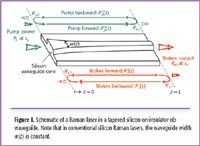
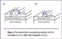
The Raman lasers considered here essentially consist of a silicon waveguide and reflectors for the Stokes (lasing) wavelength at the two ends of the waveguide, forming the laser cavity (see Figure 1). In the silicon-on-insulator (SOI) technology, silicon, with its high refractive index of about 3.5, forms the core of the waveguide (as shown in Figure 2). It is surrounded by materials of lower refractive index, typically a silica buffer layer below (refractive index of about 1.5), and silica or air above. The cavity reflectors can be formed by polished waveguide end surfaces, by thin-film coatings on the end surfaces, or by waveguide Bragg gratings. The Raman laser is pumped optically by a pump laser whose light is injected into the waveguide.
The operation principle of the laser is simple: when the pump laser at the wavelength λp is switched on, spontaneous Raman scattering will generate light at new wavelengths, the most intense peak being generated at the Stokes wavelength λs corresponding to an optical frequency downshifted by about 15.6 THz from the pump frequency. The spectral width of the Raman peak is about 100 GHz. Furthermore, any Stokes light in the cavity will be amplified through the effect of stimulated Raman scattering — it will experience Raman gain proportional to the amount of pump power. When reaching the ends of the waveguide, part of the Stokes light leaves the waveguide (forming the output beam), and part of it is reflected back into the waveguide. When the pump power is high enough, this feedback plus the amplification through stimulated Raman scattering leads to an increasing buildup of optical power at the Stokes wavelength. Eventually, a steady state is reached in which the laser continuously converts the pump radiation at λp to Stokes radiation at λs.
Nonlinear Absorption
However, there are two nonlinear absorption mechanisms that compete with the Raman gain and limit the efficiency of Raman lasing in silicon or even prevent it completely. First, even though silicon is transparent in the wavelength range of interest (λ = 1.1 . . . 5 μm), the effect of two-photon absorption (TPA) becomes noticeable at the high optical powers necessary for Raman amplification. In TPA, two photons are absorbed simultaneously, generating an electron-hole pair. The absorption caused by this effect alone does not impair the Raman-amplification process significantly. However, the increased conductivity of the silicon waveguide due to TPA-generated charge carriers leads in turn to additional optical losses called free-carrier absorption (FCA), which can indeed be substantial. The strength of FCA depends upon how much the carriers accumulate in the waveguide core before recombining. This is quantified by an effective charge-carrier lifetime τeff, which is lower when carriers quickly recombine or diffuse out of the areas of high light intensity.
The effective carrier lifetime τeff is a property of the waveguide determined by its geometry and the technological processes taken to manufacture it. If it is too high, it is impossible to make the waveguide lase. To reduce the lifetime and thus the impact of FCA, the authors in reference 1 applied a static electric field transversely across the waveguide. The field sucks the carriers out of the waveguide-core area after being generated by TPA before they can accumulate and cause significant FCA to the propagating light. The authors could indeed show that by increasing the applied electric field, the effective lifetime is decreased and lasing becomes more efficient.
On the other hand, we have recently proposed another way of increasing the efficiency of Raman amplification and lasing in silicon waveguides. By tapering — that is, varying the waveguide width along the propagation direction (as illustrated in Figure 1) — the balance between FCA and Raman gain can be adjusted optimally at each waveguide position and the net gain can be increased (13, 14). Before explaining this concept in detail, however, we have a look at the model for a standard Raman laser.
Raman-Laser Model
In our model for the steady-state characteristics of a silicon Raman laser, there are forward- (+) and backward-propagating (–) waves at the pump (p) and Stokes (s) wavelengths, the powers P± (z) of which change along the propagation direction ±z according to the differential equations (15) (see Figure 1).

Equation 1

Equation 2
At each waveguide position z, the right-hand sides of Equations 1 and 2 represent the local gain for the pump and Stokes waves, respectively, which is the sum of four terms. The first term represents the linear losses α present in every optical waveguide, for example, due to light scattering at the waveguide-sidewall roughness produced during etching. The second term describes the effect of stimulated Raman scattering (it appears as a loss to the pump waves and as a gain to the Stokes waves) with a Raman-gain coefficient g. The third term describes TPA with the TPA coefficient β. Finally, the last term gives the loss due to FCA, which is proportional to an effective charge carrier density,

Equation 3
where τeff is the effective carrier lifetime explained in the previous section. The expression for N--eff is of second order in the optical powers, because carrier generation takes place through TPA as opposed to one-photon absorption. Note that spontaneous Raman scattering does not appear in our differential equations, as its contribution is negligible once the laser has reached its steady state.

Figure 1.
An important constant appearing in Equations 1–3 is the effective area Aeff, which characterizes how strongly the waveguide confines the light. The efficiency of all nonlinear effects depends upon the intensity of light. Consequently, if the same optical power is confined to a smaller area Aeff, light intensity is higher and all nonlinear effects such as Raman scattering, TPA, and FCA are more effective (see Equations 1–3). Note in particular that the FCA term is inversely proportional to the square of Aeff.
Finally, the reflection of the Stokes (and, optionally, also the pump) waves at the two end faces of the SOI waveguide (at z = 0 and z = L) with the reflectivities R{p,s} ,{l,r} and the input coupling of the pump power P0 are taken into account by the boundary conditions

Equation 4

Equation 5
The right-hand output power of the laser is Pout = P+ (L) (1 – Rs,r).
In the boundary condition Equation 4a for pump-power injection, the injected and reflected powers simply add incoherently, because the pump-laser spectrum is so broad that it spans several free spectral ranges (FSRs) of the silicon-waveguide cavity. For example, the pump laser used in (7) is a Raman fiber laser with a spectral width of several tens of gigahertz, while a silicon-waveguide cavity with a length of 1 cm has an FSR of only c/(2Ln) ≈ 5 GHz.
Equations 1–5 have no known analytic solution and are solved numerically. Simulations presented in this article are performed for the same parameters as in (15): g = 20 cm/GW, α = 1.0 dB/cm, β = 0.7 cm/GW, and an FCA efficiency of w = 6.0 × 10⁻¹⁰ . The pump and Stokes wavelengths are λp = 1427 nm and λs = 1542 nm, respectively. We will consider only lasers that have been prepared such that they have a left-hand Stokes reflectivity of Rs,l = 100% (that is, we want to have all the laser output power on the right-hand side), whereas the other reflectivities have the reflectivity of a polished silicon–air interface of Rp,l = Rp,r = Rs,r = 30%.
Optimal Nontapered Laser
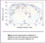
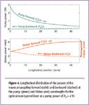
The practical question arises: What is the maximum output power we can obtain from a standard, nontapered silicon Raman laser with the parameters given at the end of the previous section? We assume that the waveguide technology has led to an effective carrier lifetime of τeff = 4.5 ns. Then the only remaining unspecified parameters are the effective area Aeff and the waveguide length L. In Figure 3, we vary these two parameters and plot the maximum output power of the resulting lasers, assuming that our pump laser is limited to 4W of power. The optimal laser, marked with a black asterisk in Figure 3, has an effective area of Aeff = 2.96 μm2 and a length of L = 45.6 mm and gives 4.3 mW of output power at the maximum available pump power of 4 W. Figure 4 shows how the pump (green) and Stokes (red) powers are longitudinally distributed inside the cavity of the optimal laser. At the left-hand side of the cavity, the amplification of the Stokes light can be seen clearly; however, toward the right-hand side, the Raman gain becomes smaller as less pump power arrives there. At the right-hand waveguide end, about 6 mW of Stokes power (solid red) are incident, of which Rs,r = 30% are reflected, forming the backward-propagating Stokes wave (dashed red). The remaining 4.3 mW are transmitted and yield the laser output power.
The most interesting aspects of the laser are its characteristics — that is, the curve showing the output power in terms of the pump power. The characteristics of the optimal laser are shown as the thin solid line in Figure 5a. The laser starts operating at a pump power of 3.1 W. Beyond this lasing threshold, the output power increases initially when the pump power is increased. Eventually, however, there is a rollover at P0 = 4.2 W and a decrease of the output power up to the shutdown threshold of 5.7 W, at which laser operation breaks down (15). This effect is due to FCA loss, which ultimately increases faster (with the square of the pump power) than the Raman gain, which increases only linearly with the pump power (see Equations 1–3).
Note that if the effective area were made smaller than the optimal value, the result would be stronger FCA and less efficient lasing due to the dependence of FCA upon the square of 1/ Aeff(see Equation 3). On the other hand, a larger effective area would lead to a strong reduction of FCA, but the Raman gain also would scale down as 1/ Aeff, so one is limited eventually by the available pump power. Consequently, there exists an optimum value for the effective area.
There also is an optimum waveguide length, because a waveguide that is too short would not provide enough interaction length for the Raman-amplification process. On the other hand, a waveguide that is too long would add an unnecessary amount of linear losses (characterized by α).
More output power could be obtained by using a waveguide with a shorter lifetime τeff, or by using a different set of mirror reflectivities. Instead of doing this, we will show next how a simple tapering of the waveguide — that is, a longitudinal variation of Aeff that can be realized by a waveguide-width variation (as illustrated in Figure 1) — can improve the characteristics by a factor of more than eight.
The Principle Behind Tapering
As discussed earlier, the onset of FCA at high pump powers limits the achievable laser efficiency. To motivate the concept of the waveguide taper, we have a closer look at Equation 2 describing the local Stokes gain at position z. Note that in the case of the optimal laser presented in the previous section, the Stokes powers are much smaller than the pump powers (see Figure 4). Furthermore, we consider for simplicity the related case in which the righthand pump reflector is Rp,r = 0, so that a backward-propagating pump wave is not present. This simplified situation corresponds to the case of a so-called undepleted single-pass Raman amplifier, where a very weak Stokes signal is amplified through stimulated Raman scattering by a strong pump signal, which is injected codirectionally (13). The Stokes gain (Equation 2) then can be written

Figure 2.
The three terms on the right-hand side of Equation 6 correspond to, respectively, linear waveguide losses, an effective Raman gain describing joint action of stimulated Raman gain and TPA loss, and FCA loss. The right-hand side should be as large as possible at each position z inside the amplifier or laser, in order to make the overall Stokes gain large and lasing most efficient.

Equation 6
It can be seen that the FCA term in Equation 6 dominates over the Raman-gain term at positions z inside the waveguide, where the pump power P+p (z) is large, because the FCA term depends on the square of the pump power. However, the FCA term also inversely depends upon the square of the effective area Aeff, whereas the Raman-gain term depends inversely upon only the first power. Consequently, by changing the value of Aeff, we can shift the relative weighting between the Raman-gain and FCA-loss terms — if FCA is too large because of large pump powers, we should increase Aeff. This would result in an undesired reduction of the Raman gain according to 1/Aeff but simultaneously in a much stronger reduction of the FCA-loss term according to 1/A2eff . Consequently, if we allow the effective area to vary longitudinally, we should simply choose Aeff (z) such that the right-hand side of Equation 6 is maximal at each waveguide position z; in other words, the balance between Raman gain and FCA is optimized at each z according to the local pump power P+p (z).
The typical shape for a taper is a decrease of Aeff toward regions of lower pump power: the latter is injected at the left-hand side (z = 0) and decreases towards the right-hand side because it loses power to the Stokes waves in the Raman-amplification process (an example for the pump-power distribution is shown in Figure 4). Therefore, the optimal effective area typically will be larger at the pumped end of the waveguide and smaller at the opposite end. However, the optimal solution for Aeff (z) is known in exact analytic form only for the case of an undepleted Raman amplifier, in which the result is that Aeff (z) should have an exponentially decaying shape along z (13). For a Raman laser, a numerical optimization of the taper is necessary (14), for which we have employed a standard genetic algorithm (16).

Figure 3.
Tapered-Laser Characteristics
In this section, we will show that the effective-area taper can indeed improve the Raman-laser characteristics. Consider first the characteristics of the optimal nontapered laser found previously under the section "Optimal Nontapered Laser," plotted as the thin solid line in Figure 5a. The corresponding "taper" (constant effective area versus waveguide position) is plotted in Figure 5b. This laser yields 4.3 mW of output power at the maximum available pump power of 4W.

Figure 4.
After the discussion in the previous section, we expect that increasing the effective area at the left-hand side of the waveguide improves the laser characteristics. The thin-dashed and dash-dotted curves in Figure 5 show two such arbitrarily chosen tapers and the corresponding laser characteristics. We did not chose any specially optimized tapers, yet both tapered lasers already produce more output power at P0 = 4 W than the best nontapered laser. Finally, the thick solid curves in Figure 5 show the results for a laser for which we have optimized the taper Aeff (z) (we have restricted the allowed effective area to the range 1 . . . 5 μm2 ) and the waveguide length L. The output power of this optimized tapered laser, 36 mW, is larger by a factor of more than eight than that of the best nontapered laser.
Note that the factor of eight is only one specific example. If the lifetime τeff of our waveguide were larger than the value we have used here (4.5 ns), the efficiency improvement from the nontapered to the tapered laser would be even larger. The most dramatic effect is obtained when τeff is so large that there simply exists no nontapered laser, and only with a taper it is possible to make the waveguide lase (14).
Conclusion
We have reviewed the operation principles of a Raman laser in a silicon waveguide. The nonlinear effect of FCA competes with stimulated Raman gain and sets an upper limit to the achievable laser efficiency. We have shown that by varying the width of the waveguide longitudinally, the balance between FCA and Raman gain can be optimized at each position inside the cavity, and thus, Raman amplification can be more efficient than in constant-width waveguides. An example calculation has shown that such a waveguide taper leads to a lasing-efficiency increase by a factor of more than eight.
References
1. H. Rong, R. Jones, A. Liu, O. Cohen, D. Hak, A. Fang, and M. Paniccia, Nature 433, 725–727 (2005).
2. L. Liao, D. Samara-Rubio, M. Morse, A. Liu, D. Hodge, D. Rubin, U.D. Keil, and T. Franck, Opt. Express 13(8), 3129–3135 (2005).
3. Q. Xu, B. Schmidt, S. Pradhan, and M. Lipson, Nature 435, 325–327 (2005).
4. Y.A. Vlasov and S.J. McNab, Opt. Express 12(8) 1622–1631 (2004).
5. G.T. Reed, Nature 427, 595–596 (2004).
6. L. Pavesi and D.J. Lockwood, Eds. Silicon Photonics (Springer-Verlag Berlin Heidelberg, 2004).
7. R. Claps, D. Dimitropoulos, V. Raghunathan, Y. Han, and B. Jalali, Opt. Express 11(15), 1731–1739 (2003).
8. R.L. Espinola, J.I. Dadap, J. Richard M. Osgood, S.J. McNab, and Y.A. Vlasov, Opt. Express 12(16), 3713–3718 (2004).
9. Q. Xu, V.R. Almeida, and M. Lipson, Opt. Express 12(19), 4437–4442 (2004).
10. T.K. Liang and H.K. Tsang, Appl. Phys. Lett. 85(16), 3343–3345 (2004).
11. V. Raghunathan, R. Claps, D. Dimitropoulos, and B. Jalali, J. Lightwave Technol. 23(6), 2094–2102 (2005).
12. O. Boyraz and B. Jalali, Opt. Express 12(21), 5269–5273 (2004).
13. H. Renner, M. Krause, and E. Brinkmeyer, "Maximal Gain and Optimal Taper Design for Raman Amplifiers in Silicon-on-Insulator Waveguides," in Integrated Photonics Research and Applications Topical Meeting (IPRA), 2005, paper JWA3.
14. M. Krause, H. Renner, and E. Brinkmeyer, "Efficiency increase of siliconon-insulator Raman lasers by reduction of free-carrier absorption in tapered waveguides," in Conference on Lasers and Electro-Optics (CLEO), 2005, paper CThB 1.
15. M. Krause, H. Renner, and E. Brinkmeyer, Opt. Express12(23), 5703–5710 (2004).
16. J. Lampinen, A Bibliography of Differential Evolution Algorithm, Lappeenranta University of Technology, Department of Information Technology, Laboratory of Information Processing, 2001, available via Internet:
http:// www.lut.fi/ jlampine/debiblio.htm.
Michael Krause,Hagen Renner, and Ernst Brinkmeyer are with Technische UniversitE4t Hamburg-Harburg (Hamburg, Germany; http://www.om.tu-harburg.de). E-mail: m.krause@tu-harburg.de

AI-Powered SERS Spectroscopy Breakthrough Boosts Safety of Medicinal Food Products
April 16th 2025A new deep learning-enhanced spectroscopic platform—SERSome—developed by researchers in China and Finland, identifies medicinal and edible homologs (MEHs) with 98% accuracy. This innovation could revolutionize safety and quality control in the growing MEH market.
New Raman Spectroscopy Method Enhances Real-Time Monitoring Across Fermentation Processes
April 15th 2025Researchers at Delft University of Technology have developed a novel method using single compound spectra to enhance the transferability and accuracy of Raman spectroscopy models for real-time fermentation monitoring.
Nanometer-Scale Studies Using Tip Enhanced Raman Spectroscopy
February 8th 2013Volker Deckert, the winner of the 2013 Charles Mann Award, is advancing the use of tip enhanced Raman spectroscopy (TERS) to push the lateral resolution of vibrational spectroscopy well below the Abbe limit, to achieve single-molecule sensitivity. Because the tip can be moved with sub-nanometer precision, structural information with unmatched spatial resolution can be achieved without the need of specific labels.