How to Design a Miniature Raman Spectrometer
Special Issues
In this article, we describe the key factors that influence the overall size of a spectrometer, such as the diffraction grating groove density and detector size. Furthermore, we demonstrate compact Raman spectrometer designs as small as 30 mm × 30 mm in footprint by using highly dispersive gratings and uncooled detectors.
In this article, we describe the key factors that influence the overall size of a spectrometer, such as the diffraction grating groove density and detector size. Furthermore, we demonstrate compact Raman spectrometer designs as small as 30 mm × 30 mm in footprint by using highly dispersive gratings and uncooled detectors.
Raman spectroscopy (1) has been around for many years and is being used as one of a multitude of molecular spectroscopic techniques. The typical Raman spectrometer is a large and expensive benchtop instrument with very high performance. Such instruments are typically for general-purpose laboratory use and, therefore, need to be flexible in the choice of Raman shift range and resolution through configuration with different lasers and gratings. Also, the required resolution can be as low as 1 cm-1.
Recently, Raman instruments have been introduced that are dedicated to specific applications like security screening for hazardous materials (2) and incoming inspection of raw material in the pharmaceutical industry (3). These applications have been enabled by the compact size, lower cost, and reduced power consumption of such dedicated Raman instruments.
In contrast to the benchtop, high performance, laboratory Raman systems, the dedicated instruments only need to cover a fixed wavelength range, and the resolution requirement is often relaxed, since the spectral features to look for are known in advance. As an example, many systems use a 785-nm laser and a 800–1100 nm spectrometer, which will provide a Raman shift range from 200 cm-1 to 3650 cm-1 with a resolution of 10–20 cm-1.
The main enabler for these compact Raman instruments has been the development of ultracompact, high-power, and low-cost semiconductor lasers (4). However, miniaturization of the spectrometer is also an important factor.
In this article, we describe the key factors that influence the overall size of a spectrometer, such as the diffraction grating groove density and detector size. Furthermore, we demonstrate compact Raman spectrometer designs and share some experimental results.
Theory of Raman Spectrometer Design
Based on the key spectrometer parameters defined in Figure 1, we will discuss how these parameters influence the overall size of the spectrometer. The basic theory for a spectrometer design can be found in Neumann's book (5).
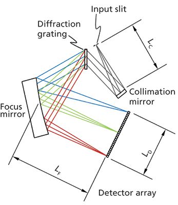
Figure 1: Schematic diagram of diffractive spectrometer with definitions of relevant parameters: LC = focal length of collimation mirror; LF = focal length of focus mirror; LD = length of detector.
Light enters at the input slit and is collimated into a parallel bundle of rays by the collimation mirror. The grating diffracts the different wavelengths λ of the input light into different angles β(λ) as given by the grating equation:

Where G is the grating groove density and α is the angle of incidence on the gratings. The focusing mirror focuses the different wavelengths in different positions on an array of photodetectors-often a charge-coupled device (CCD) or complementary metal–oxide–semiconductor (CMOS) type array.
Next, we use examples from practical limitations and requirements of Raman spectroscopy to demonstrate how ultracompact spectrometers can be designed.
Focal Length
One of the key parameters for the overall spectrometer size is the focal length of the two mirrors or lenses in the spectrometer. Equation 2 gives a good estimation of how the focal length of the focusing mirror (LF) is related to the length of the detector (LD), the grating groove density G, and the wavelength range (λ2 – λ1) that needs to be covered:

From Figure 1 it can be seen that the size of the spectrometer scales with the focal length, so to obtain a compact spectrometer the focal length should be minimized. The wavelength range is typically given by the application and is not a design parameter. For instance, if the laser wavelength is 785 nm and the fingerprint region 200–3650 cm-1 is to be measured, the wavelength range must be 800–1100 nm. From equation 1 it can be seen that the focal length can be minimized by choosing a grating with a high groove density G or a short detector length LD. β is the diffraction angle for the center wavelength (950 nm in the example above) and is dependent on G as seen from equation 1, however the cosine term cos(β) is a slowly varying function of G. In practice, the commercially available detectors are typically either ¼-in., ½-in., or 1-in. wide. Grating groove densities typically vary from 300 lines per mm (l/mm) to 1800 l/mm for the wavelength range of interest.
In Figure 2 we have plotted the focal length of the focusing mirror as a function of the grating groove density for ¼-in., ½-in., and 1-in. detectors covering the 800–1100 nm wavelength range. The graph clearly shows that there are nearly two orders of magnitude in difference between the largest spectrometer design (300 l/mm grating and 1-in. detector) and the smallest spectrometer design (1800 l/mm grating and ¼-in. detector).
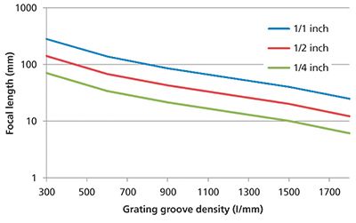
Figure 2: Focal length of focus mirror (LF) as a function grating groove density and detector size. Wavelength range: 800–1100 nm.
Numerical Aperture
Another important parameter that influences the size of a spectrometer is the numerical aperture or f-number. As shown in Figure 3, the numerical aperture of the spectrometer is the sine of the cone of angles that the spectrometer accepts as input. The larger the numerical aperture, the more light can be coupled into the spectrometer. However, the numerical aperture will also determine the width of the beam going through the spectrometer and thereby the size of all the optical elements inside. This means that a compromise often has to be made between compact size and high throughput.
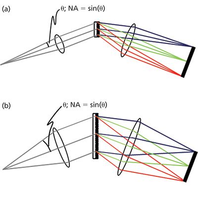
Figure 3: Size of spectrometer for the case of (a) a low numerical aperture and (b) a high numerical aperture.
Resolution
The resolution of a spectrometer defines the ability to resolve closely spaced features in the spectral domain (measured in nanometer or wavenumber). Raman spectra often exhibit closely spaced peaks and for this reason spectrometers with high resolution are required. However, the resolution will also influence the size of the spectrometer as will be explained in this section.
The resolution of the spectrometer is determined by the following two factors:
- Pixel resolution: The number of pixels covering the spectral range.
- Optical resolution: The image of the input slit on the detector.
Pixel Resolution
The more pixels the detector has, the better the resolution, as seen from the example in Table I. However, more pixels generally also means a wider detector, which again means a larger spectrometer as explained previously. Because the smallest pixel spacing of scientific CCDs is typically in the 10–12 µm range, one can say-as a rule of thumb-that 2048 pixels corresponds to a 1-in. detector while a 512-pixel detector corresponds to a ¼-in. detector. Typically, a peak needs to be sampled by a minimum of 2–3 pixels to determine the peak center accurately. As mentioned in the introduction, process Raman typically requires ~10 cm-1 resolution, so with a 1024-pixel detector (4.5 cm-1/pixel sampling as seen from Table I) we should be able to obtain the required resolution. If the resolution requirement is 20–25 cm-1, we can even reduce the number of pixels to 512.

Optical Resolution
The optical resolution of the spectrometer is determined by the input slit size and the optics inside the spectrometer. The best possible resolution that can be obtained is the diffraction limit, which is the resolution obtained with an infinitely small input slit. The diffraction limit is related to the size of the beam width inside the spectrometer. For instance, equation 3 determines how the beam width on the grating wbeam limits the resolution ΔλFWHM:

The wider the beam, the more grating lines the beam illuminates and, therefore, the better the resolution. This is also referred to as the resolving power of the grating.
Signal-to-Noise Ratio
In Raman spectroscopy, the optical signal levels are very weak. Since the CCD detectors are capacitive, the electrical signal level can be increased by integrating for a long time-often several seconds. The drawback of this approach is that the noise of the CCD also increases with a long integration time. Therefore, it is quite common to cool the detector to lower the detector noise level.
For compact spectrometers, it is often desirable that they are battery operated, since the instrument should be portable. This requires that the electrical power consumption of the instrument is low, which can be obtained if the detector is uncooled.
As written above, if cooling is to be avoided, the integration time has to be short and thereby the signal level as high as possible. Therefore, it becomes important to use few, yet efficient optical elements in the spectrometer to increase the optical throughput.
Experimental Results
In this section, we describe the results obtained using compact spectrometers that we have designed following the general guidelines described above. We wanted a spectrometer that covered 800–1100 nm with a resolution of 0.6 nm, corresponding to 9 cm-1 at 800 nm. We also wanted to use a noncooled detector, so we chose to use transmission gratings with very high diffraction efficiency.
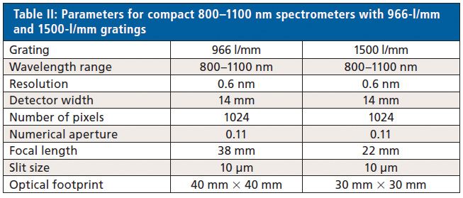
Table II lists the key parameters for two spectrometer designs we have made, and Figure 4 shows the optical designs on a relative scale. Both spectrometers have a numerical aperture of 0.11. To compare the relative size of the two spectrometers, we have indicated the footprint of the optical beam paths in Figure 4. As can be seen, the footprint is 40 mm × 40 mm with the 966-l/mm grating and reduces to only 30 mm × 30 mm with the 1500-l/mm grating. Obviously, the footprint will be 10–15 mm larger on each side to allow for the size of the mirrors and housing around the spectrometer.
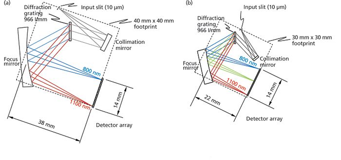
Figure 4: 800–1100 nm spectrometer designs: (a) 966-l/mm grating with a footprint of 40 mm × 40 mm and (b) 1500-l/mm grating with a footprint of 30 mm × 30 mm.
To experimentally verify our design work, we built a spectrometer with the 966-l/mm transmission grating and tested it. From Table I, we chose to use a 14-mm-wide noncooled back-thinned (BT)-CCD detector with 1024 pixels of 14 µm pixel-to-pixel spacing, which has enough pixels to resolve a peak with a full width at half maximum (FWHM) of 0.6 nm. The mirrors were spherical mirrors. The spectrometer was designed for a theoretical resolution of 0.5 nm using a 10-µm-wide slit, since we expected the experimental resolution to be somewhat larger than the theory.
After assembling and aligning the spectrometer, we measured the resolution versus wavelength. We used spectral lines from an argon lamp (see reference 6 for details), which all had very small linewidths, such that the measurements were not disturbed by the lamp itself.
The measured resolution is shown with diamond marks in Figure 5. As shown in the figure, the resolution is very close to the desired 0.6 nm across the full range except close to 1100 nm. The solid line in Figure 5 is the theoretical resolution calculated numerically using ray-tracing. The measurements are in good agreement with the theory, taking into account the tolerances of alignment and optical mirror curvatures. The overall footprint including mirrors and mounts for this spectrometer were approximately 60 mm × 60 mm × 20 mm.
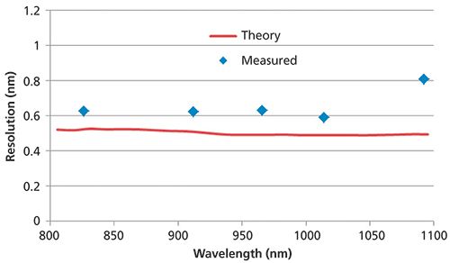
Figure 5: Measured resolution of the 800–1100 nm spectrometer. The solid line is the theoretically calculated resolution.
Summary
In summary, we have shown that the key parameters determining the size of a spectrometer are the grating groove density, the detector width, and the numerical aperture. To design a compact spectrometer, the grating groove density should be as high as possible and the detector and numerical aperture as small as possible. We also discussed that the desired resolution of the spectrometer will ultimately set a limit to how small the design can be. Also, the numerical aperture will likely have to be a compromise between high throughput and small size. We designed two spectrometers, one with a 966-l/mm grating and one with a 1500-l/mm grating, and showed that the design can be as small as 30 mm × 30 mm. Furthermore, we built a spectrometer using a 966-l/mm transmission grating. This spectrometer covered the full 800–1100 nm range, and we measured the resolution to be 0.6 nm across almost the complete range. Such a spectrometer could be as small as 60 mm × 60 mm × 20 mm and is applicable for a portable Raman system with a 785-nm laser, thereby providing coverage of the 200–3650 cm-1 range with better than 10 cm-1 resolution.
Thomas Rasmussen, Michael Rasmussen, Poul Hansen, Ole Jespersen, Nicolai Rasmussen and Bjarke Rose are with Ibsen Photonics in Farum, Denmark. Direct correspondence to: thomas.rasmussen@ibsen.dk
References
(1) D.J. Gardiner, Practical Raman Spectroscopy (Springer-Verlag, Berlin, Germany, 1989).
(2) P. Loeffen, G. Maskall, S. Brontron, M. Bloomfield, and C. Tombling, Proc. SPIE 8018, 80818E (2011).
(3) P. Matousek, F. Thorley, P. Chen, M. Hargreaves, C. Tombling, P. Loeffen, and M. Bloomfield, Spectroscopy 26, 44–51 (2011).
(4) B.L. Volodin, S.V. Dolgy, E.D. Melnik, E. Downs, J. Shaw, and V.S. Ban, Opt. Lett. 29, 1891–1893 (2004).
(5) W. Neumann, Fundamentals of Dispersive Optical Spectroscopy Systems (SPIE, PM242, 2014).
(6) A. Kramida, Y. Ralchenko, J. Reader, and NIST ASD Team. NIST Atomic Spectra Database (Ver. 5.2), (online). Available at: http://physics.nist.gov/asd (January 22, 2015), (National Institute of Standards and Technology, Gaithersburg, Maryland, 2014).
AI-Powered SERS Spectroscopy Breakthrough Boosts Safety of Medicinal Food Products
April 16th 2025A new deep learning-enhanced spectroscopic platform—SERSome—developed by researchers in China and Finland, identifies medicinal and edible homologs (MEHs) with 98% accuracy. This innovation could revolutionize safety and quality control in the growing MEH market.
New Raman Spectroscopy Method Enhances Real-Time Monitoring Across Fermentation Processes
April 15th 2025Researchers at Delft University of Technology have developed a novel method using single compound spectra to enhance the transferability and accuracy of Raman spectroscopy models for real-time fermentation monitoring.