Miniature Optical Spectrometers: The Art of the Possible, Part IV: New Near-Infrared Technologies and Spectrometers
Part II of this series described many of the miniature optical technologies that were developed as a result of the telecommunications boom, and Part III covered conventional small near-infrared (NIR) spectrometers. Here, in Part IV, we bring those themes together and see how the massive investment in telecommunications, microelectro- mechanical systems (MEMS), and micro-opto-electro-mechanical (MOEMS) is starting to impact NIR spectroscopy.

Here in Part IV, we will cover new spectrometer fabrication techniques, new light sources, and wavelength-selective devices. Researchers are combining new wavelength-selective devices with focal plane arrays to produce tunable arrays, and photonics technology is enabling new classes of multiplex spectrometers, based upon Hadamard transform techniques. So we are looking at "the art of the possible" (4): what new spectrometers can be constructed, and how they can be constructed, using all the technologies developed during the 1990s. In particular, many new NIR technology developments employ Fabry–Pérot tunable filters, the theory and properties of which were described in Part II of this series (1). We will concentrate on spectrometers made possible by micro electro mechanical systems (MEMS), micro-opto-electro-mechanical systems (MOEMS), and LIGA technologies. Some other interesting developments are omitted, but should be noted: slab waveguide spectrometers (5–9); handheld tunable diode laser absorption spectrometers (TDLAS) (10); a biomedical, in-vivo, scanning spectrometer (11); linear variable filters (12); fixed-filter instruments based upon spectroscopic principal components (13,14); developments in NIR array detector technology (15,16); a macroscopic tunable Fabry-Pérot filter coupled to a focal plane (17); and Fourier-transform (FT)-IR spectrometers using photoelastic modulators (18) and liquid crystals (19) to provide optical path differences, just to name a few.
Spectrometer Fabrication
LIGA
LIGA (20–23) is a German acronym for X-ray lithography (Lithographie), electroplating (Galvanoformung), and molding (Abformung), and this technology was described in Part II (1). A number of spectrometers have been fabricated using the LIGA process. They fall into two classes: first, those in which the metal LIGA parts are used directly in the spectrometer, and second, those in which the metal LIGA parts are used as the master mold for a plastic-body spectrometer.
A LIGA NIR FT spectrometer has been described (24–26), in which the whole optical system fits on a chip with dimensions of 11.5 mm × 9.4 mm. The structural components of the spectrometer were fabricated in an iron-nickel (FeNi) alloy, as were the plunger and microcoil cores of the drive mechanism and the fiber-optic mounts. The mirrors were also FeNi structures, made by LIGA. The beamsplitter, detector, and lenses were commercially available optical components. A mirror travel of about 300 μm was planned, but in practice, only 54 μm was achieved, with a resolution of about 25 nm.
LIGA has been used in the manufacture of visible and NIR spectrographs, by production of a nickel master molding tool, and then hot-embossing polymethylmethacrylate (PMMA) (27,28). These are monolithic, hollow, "slab-waveguide" spectrometers (Figure 1). The UV–vis and NIR spectrometers from microParts share the same design principle and production process (29). These designs are based upon a monolithic spectrometer chip, which contains all the optical components — entrance slit, self-focusing echelette diffraction grating, and deflection mirror — all on a single injection-molded part. A reflective coating (aluminum in the NIR and gold in the UV–vis) is deposited on the chip. The UV–vis spectrometers use a 256-pixel detector and cover the range of 350–1050 nm at <10-nm resolution, while the NIR version is equipped with an InGaAs array detector and covers 1000–1700 nm at <16-nm resolution. The NIR spectrometer module is 61 mm × 42 mm × 16 mm in size.

Figure 1
A second spectrometer, also fabricated by LIGA precision injection molding, operates in the visible and short wavelength NIR (30). With a 256-pixel detector, the NIR version covers 740–1050 nm at <8-nm resolution. The size of this "spectrometer engine" is 41 mm × 21 mm × 26.5 mm. The use of LIGA to produce a master mold, and subsequent hot-embossing or precision injection molding, leads to a lower-cost manufacturing technique as compared with conventional assembly processes. The microParts UV–vis spectrometer described earlier can sell for less than $400 in very large quantities (29). LIGA spectrometers of this type have found a number of diverse, dedicated applications, principally in the visible region; for instance, in noninvasive measurement of newborn jaundice (31), measurement of blood parameters (32), and color grading of diamonds (33).
Sources
Semiconductor Light Sources
As we have seen (2), light-emitting diodes (LEDs) can be used as sources in NIR spectrometers, but a variety of enhancements can improve their utility. Adding an optical waveguide region, consisting of a ridge structure on the LED's upper surface, will guide the emitted light by total internal reflection, and allows efficient coupling of that light into small optical fibers. A super luminescent light-emitting diode (SLED) is a ridge-waveguide light-emitting diode, pumped at high current levels so that stimulated emission occurs, enhancing emission into the waveguide (34). A SLED is not a laser, and precautions are taken to prevent lasing; typically, the rear of the device is not electrically pumped, and light suffers both absorption and diffraction in this "lossy" region, preventing the formation of a resonant cavity. Figure 2 shows a SLED on a miniature optical bench, with its emission coupled into a miniature GaP lens, mounted on a metal LIGA alignment structure.
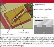
Figure 2
SLED light sources are available commercially from a number of vendors (35) in the traditional telecommunications region of the spectrum (O-, C-, and L-bands), and also can be fabricated for use at longer wavelengths. A typical SLED has an emission width of 60–100 nm; therefore, they fall into an intermediate area in which they are not broadband enough for an individual SLED to be a general purpose source, nor are they narrow enough to be a useful spectroscopic sensor on their own. An additional wavelength-selective device is required, and Axsun Technologies' (36) first analytical spectroscopic instruments were "tunable-SLEDs" (T-SLEDs), coupling a SLED to a MEMS Fabry-Pérot tunable filter, and based partially on their earlier telecommunications optical channel monitor (OCM) products (37–40).
The optics for the T-SLED are on a 14-mm long miniature optical bench, itself contained in a 14-pin, chip-sized butterfly package (Figure 3). This level of integration is made possible by a number of MEMS components and techniques: SLED sources, miniature lenses made by a mass-transport process, a MEMS Fabry–Pérot tunable filter, broadband high-reflectivity coatings, LIGA-fabricated optical mounts, and a robotic active-alignment process (37). One key step is reducing the problem of miniature optical assembly to one that has been solved already: placement and laser soldering of miniature electronic components onto printed circuit boards using pick-and-place machines.

Figure 3
The MEMS tunable Fabry–Pérot filter (Figure 4) consists of two mirrors, facing each other and separated by a few micrometers. Changing the mirror separation by applying voltage to the MEMS structure tunes the transmitted wavelength (1). Because of the extremely small size and low mass of the movable mirror, the mechanical resonant frequency of the filter is over 100 kHz, and it can be scanned physically over its entire range in less than 50 μs (36,37). These optical filters address the issues raised in a 2004 paper (41) that commented that the resolution (expressed as R = Δλ/λ) of a miniature Fabry–Pérot filter would be limited to ~30; these spectroscopy designs commonly achieve ~1500, and telecommunications designs achieve considerably higher than that.
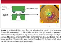
Figure 4
The T-SLED spectrometer concepts were developed further to make a broadband tunable laser. A laser typically consists of a cavity formed by two mirrors, containing a gain medium and a wavelength-selective element. Construction of this laser was achieved by taking the optical components described for the T-SLED spectrometer, but substituting a semiconductor optical amplifier (SOA) for the SLED, using the tunable Fabry–Pérot filter in the cavity as the wavelength-selective element. An SOA is pumped along its full length, in contrast to a SLED, and light is emitted from both ends. With a typical SOA, lasing is achieved over a ~200 nm range, with a resolution of ~1 nm and a power of ~1 mW. They offer three ranges (1350–1550 nm, 1550–1800 nm, and 1800–1970 nm), and these can be combined in a single spectrometer to cover 1350–1970 nm.
Axsun has delivered spectrometers for a number of process pharmaceutical applications, including active pharmaceutical ingredient drying (42) and blend monitoring (43), while both Axsun and Polychromix have developed portable dedicated instruments for carpet and plastic recycling (44,45). Process applications are demanding (46,47), and miniature instruments (48) have some potential advantages in that environment. In particular, the resonant frequency of a MEMS device can be very high, in the tens of kilohertz, implying that they will be unaffected by the usual low-frequency vibrations (tens to hundreds of hertz) encountered in a process environment. In the case of pharmaceutical blend monitoring (49), a battery-powered spectrometer is mounted on the lid of the rotating (10–15 rpm) intermediate bulk container, viewing its contents through a flush-mounted sapphire window. It communicates via wireless, and obtains a 2-nm-resolution spectrum, with noise less than 0.04 mAU, in about 400 ms on every rotation as the container passes through its inverted position.
Recycling of carpet fibers (50), plastics, and polymers, while in existence for some time, has seen significant growth driven by a combination of increasing regulation, escalating disposal costs, rising feedstock prices, and the rapid expansion of economies in China and India. Typical carpet fibers are polyethylene terephthalate (PET), polypropylene (PP), Nylon 6 (N6, polycaprolactam), Nylon 66 (N66, formed from hexamethylenediamine and adipic acid), and wool; these can be recycled if the facility can identify and separate these materials rapidly. In recent years, many outlets have been developed for these recycled resins; for instance, polypropylene is used in leachfield drainage chambers (51) and "plastic lumber" products such as fence posts, decking, and railroad ties (52), while Nylon 6 can be depolymerized back to caprolactam (50). Carpet recycling, therefore, has multiple benefits: less material in landfills, lower consumption of petroleum feedstocks, and economically viable production of industrial and consumer products (53). Identification of these materials typically is performed in a sorting facility by unskilled personnel, and frequently in a hot, humid, dusty industrial environment. This market has been addressed by both Axsun and Polychromix, with dedicated, battery-powered, MEMS-based, portable spectrometers (44,45). These are "material identification" instruments — their primary output is not the display of a spectrum, but the name of the material, via an audio output, as well as visual — and are the first widespread applications of analytical MEMS-based NIR spectrometers, with about 200 instruments deployed in 2007.

Figure 5
MEMS Gratings
MEMS optical scanning technology enables rotation of miniature gratings (Figure 5) using a comb drive, and thus a miniature scanning spectrometer (Figure 6). This concept has been realized (54,55), and a series of spectrometer "engines" has been described (56). The 2 mm × 2 mm grating, with 500 lines per mm, is fabricated by deposition of aluminum on the silicon substrate of a scanning mirror, followed by plasma etch through a photo mask, and the complete scanning grating assembly is placed in a standard 14-pin butterfly package. The scanning grating is resonantly driven; that is, it oscillates at its natural resonant frequency, and this also means that its motion approximates that of a simple harmonic oscillator, with a sinusoidal velocity profile. The spectrometer covers the range 1.2–1.9 μm with a resolution of about 10 nm, and a single-element InGaAs detector is used. The size of the complete engine (with electronics and so forth) is 100 mm × 80 mm × 75 mm.
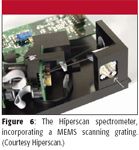
Figure 6
A conventional NIR fixed-grating spectrograph (2), equipped with a linear InGaAs array detector, enjoys a multichannel advantage, collecting every resolution element in the spectrum simultaneously, and 512-element arrays are now common. However, this MEMS-grating spectrometer scans sequentially, ceding that multichannel, and thus signal-to-noise ratio (S/N), improvement. Its potential advantage is in lower-cost fabrication, essentially replacing a relatively expensive InGaAs array detector with a potentially low-cost MEMS scanning grating in applications in which the reduced S/N (for a given measurement time) is acceptable.
Tunable Array Detectors
Two-dimensional NIR array detectors, based upon InGaAs, indium antimonide (InSb), and mercury–cadmium–telluride (MCT or HgCdTe), have been available for many years and, in analytical applications, are employed widely in spectroscopic imaging (57). Recent developments in cameras, and in the integration of MOEMS devices with cameras, might impact NIR spectroscopy.
Researchers at the University of Western Australia (Perth, Australia) have described the integration of MEMS optical filters with two-dimensional MCT-array detectors (58–62). This is based upon fabrication of MEMS-tunable Fabry–Pérot filters (Figure 7) (63) over each pixel in the MCT array, in a monolithic structure, and the goal is to produce low-cost, single-detector spectrometers and high-density, integrated imaging arrays. These devices could have low power consumption and low weight, be easy to cool, and be available in handheld packages, and the resulting spectroscopic imager could be the same size as today's CCD cameras. However, this approach does involve several significant challenges.
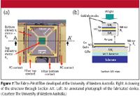
Figure 7
MCT arrays do not tolerate the high temperatures of many semiconductor fabrication processes as a result of the volatility of mercury. Therefore, low-temperature (<100 °C) processes for the Fabry–Pérot construction must be employed. In addition, their goal is to move to mid-infrared (MIR) wavelengths, and this means that both the Fabry–Pérot cavity length and the mirror displacement must be larger than those employed for NIR applications. Recent work (64) reports on a tunable MEMS filter monolithically integrated on an MCT detector: a fully integrated filter with a center wavelength of 1950 nm gave a full width at half maximum (fwhm) of approximately 100 nm, with a tuning range of 400 nm.
This group also has applied this concept to a single-element detector system, the goal being a rugged spectrometer for both agricultural and petrochemical applications. Figure 8 shows a drawing of a MEMS Fabry–Pérot tunable filter mounted over a detector, with this tunable detector packaged into a standard TO-8 can (62). A preliminary device was designed to operate between wavelengths of 1.6 μm and 2.3 μm, with a 1.2 μm spacing between the Fabry–Pérot mirrors. Although a 30-nm resolution was planned, only 100 nm was achieved as a result of mirror curvature. Mirror "snap-down" can be an issue in miniature Fabry–Pérot devices. This refers to nonlinear behavior in the voltage-displacement curve, where the moving mirror is attracted to a static element and can become permanently "stuck" due to the very strong Van der Waals forces that occur on this physical scale. This group is addressing both of these issues in new device designs.
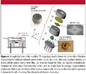
Figure 8
A number of companies (including Polychromix and Aspectrics), using different technologies, are working in the ~1300–2750 nm range, covering the first overtone (O-H, N-H, and C-H) and combination spectral regions. Extended InGaAs arrays can cover to ~2400 nm, and PbS and PbSe arrays have been used at longer wavelengths. However, the use of MCT arrays has been proposed for this region by researchers at VTT, Finland (65). In contrast to the use of MCT detectors in the MIR, where they require cooling to 77 K, operation at 200 K is sufficient for a 3-μm cutoff, and this can be achieved with a three-stage Peltier (thermoelectric) cooler. VTT has developed a photoconductive linear MCT array, 128 × 1 pixels, 1800 μm × 80 μm in size, with a 100-μm pitch. This has a new readout design, which uses synchronous (that is, lock-in) detection for each of the channels, and the detector achieves a detectivity (D*) of 1.5 × 10¹¹ . It requires a chopped light source (800 Hz was employed), which allows discrimination against ambient light, including fluorescent illumination. The complete detector package, including Peltier cooler, has a footprint of approximately 6 cm × 5 cm. VTT has developed a demonstration spectrometer, incorporating this detector, with eight parallel A/D converters, each running at 250 kHz, with the lock-in detection implemented in software running on a PC. Because of the nature of MCT material, this approach can be extended to longer wavelengths.
Multiplex Spectrometers
Fourier Transform
Some MEMS-based FT spectrometers were described in Part I of this series (2), but we will revisit that area briefly. Kraft and colleagues (66) have described a number of miniaturized spectrometers, including a spectrometer with a MEMS interferometer (67–70). This employed a resonantly driven micromirror that is suspended on two long springs, driven by interlocking comb-structured electrodes, and contained in a vacuum chamber. The effective mirror area was ~1.6 mm2. The first prototype covered a spectral range of ~4500–1450 cm–1, using a thermoelectrically cooled MCT detector, at a spectral resolution of better than 30 cm–1, and a wavelength stability of better than 4 cm–1. It had a footprint of 180 mm × 120 mm × 120 mm and a weight of about 1.5 kg, and has now been commercialized (71), covering the 2–6 μm range at 30 cm–1 resolution. However, the developers found that the moving mirror suffered from a physical distortion (72), and a "pantograph" moving mirror (Figure 9) has now been designed, which also has a larger mirror area (7 mm2). These mirrors also are driven at their resonant frequencies, similar to the scanning grating described earlier. Again, this leads to a sinusoidal mirror velocity profile, in contrast to the efforts made in laboratory FT-IR spectrometers to achieve as uniform a mirror velocity as possible (73). The limited mirror displacement available in most MEMS implementations leads to thoughts of increasing this by various means; for instance, a "Genzel interferometer" (74) uses both sides of the moving mirror to double the optical retardation for a given physical mirror displacement. Alternatively, more than one moving mirror could be used together; however, MEMS devices will not have exactly the same resonant frequencies, which could lead to dephasing of the mirror motions. The goals of the IPMS/CTR team are to have a third generation spectrometer with an optical path difference of 1 mm, capable of 1-ms time resolution, in a package that is 50 mm × 50 mm × 50 mm.

Figure 9
Hadamard
A Hadamard spectrometer (75–77) is a multiplex device; that is, it observes more than one wavelength at a time. This translates into improved S/N (or shorter measurement times) if the measurement is detector-noise limited. Given the brightness of NIR sources, and the low noise levels of NIR detectors, many NIR measurements are shot-noise limited, not detector-noise limited. However, detectors are noisier when the coverage extends to longer wavelengths, for instance beyond the 1.7-μm cutoff for "standard" InGaAs material. In addition, light levels are low, and large area detectors are beneficial for diffuse reflectance measurements in the combination region. In those cases, the measurements can be detector-noise limited, and therefore a multiplex technique is advantageous.
A Hadamard spectrometer uses one or two masks, instead of slits. Harwit and Sloane (75) gave a detailed analysis of the possible types of Hadamard spectrometers and their theoretical S/N advantages. Because new technologies are enabling a new generation of Hadamard spectrometers, a highly simplified summary will be given here. Figure 10 (top) shows a version of a one-mask and a two-mask Hadamard spectrometer. In the single-mask design shown, light passes from the source through a sample and onto the entrance slit of a spectrograph. It is dispersed by a grating, and then the encoding mask selects 50% of the resolution elements and passes that light onto a single element detector. A typical mask is an array of zeros and ones, either allowing or not allowing the light to pass onto the detector. The position of the zeros and ones in the mask changes, and the detector is read out for each of these positions. Typically, the mask uses a cyclic "S-matrix" sequence, in which each row is obtained by shifting the previous row one place to the left, shown below for a 7 × 7 case (75):

At the end of data collection, a simple matrix transform recovers the spectrum from the collected data. Typical commercial spectrometers use 128 resolution elements. In a single-mask system, the theoretical S/N gain is ½√n, where n is the number of resolution elements; for 128 elements, this equals ~5.6. In NIR, one practical point is that this advantage can be gained using a low-cost, single element detector, as opposed to a relatively expensive array detector.
Figure 10 (bottom) shows a simplified dual-mask implementation. In this case, an entrance mask is used, giving a throughput advantage over an entrance slit, and a two-dimensional array detector acts as the second mask. In a 1993 paper (78), this design was applied to the weak emission from applications such as aurora spectroscopy, which were detector-noise limited, even with a CCD detector. The authors noted that the technique assumes that the coded aperture mask (entrance aperture) is illuminated uniformly, at least in the dispersion direction: this is a key caveat with important sampling consequences for analytical spectrometers. Today, the combination of array detectors and MOEMS devices enable the fabrication of doubly encoded Hadamard spectrometers in many spectral regions (79). A Hadamard-type, doubly encoded spectrometer design has been described recently (80–82), using a stationary mask, and having applications for weak signals (for example, Raman spectroscopy [83,84]) or large diffuse sources (85–87). At present, this technique is being applied mostly in Raman spectroscopy and will not be discussed in detail here.
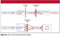
Figure 10
Returning to single-mask designs, the spectrometer from Aspectrics (88) was described in Part I (89), and this can be thought of as a Hadamard device using a sinusoidal mask, as opposed to a binary (on/off or zero/one) mask; alternatively, it can be thought of as a Fourier transform spectrometer using a rotating disk modulator instead of a Michelson interferometer. In the NIR, this spectrometer is configured to cover 1375–2750 nm, with 128 channels, using a quartz halogen source and a single-element PbSe detector. It can acquire 100 scans per second.
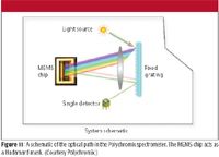
Figure 11
Polychromix (90) has produced a handheld NIR spectrometer, using a MEMS chip as the Hadamard encoding device (91). Figure 11 shows the single-mask-style optical design. The Hadamard mask is a programmable MEMS diffraction grating (92–94), originally developed as the key element in a programmable correlation spectrometer for remote detection in the MIR (3–5 μm), with the ability to create "synthetic spectra" (95). The MEMS grating consists of a parallel set of reflecting ribbons, with individual rectangular pixels 20 μm wide and 1 cm long, which can be deflected vertically while remaining planar (Figure 12). With the telecommunications boom, this was adapted for use in the C-band (around 1550 nm) as the key element in a reconfigurable optical add drop multiplexer (ROADM) for dense wavelength division multiplexing (DWDM) applications. With the telecommunications bust, it was then applied to analytical NIR spectroscopy.

Figure 12
The light from the sample is dispersed across the MEMS device, acting as a Hadamard mask. By deflecting a pixel or groups of pixels a distance of one fourth of the wavelength of incident light, that light will suffer destructive interference and be directed away from the recollimation optics. It is possible to operate the spectrometer in a number of different modes: monochromator, one wavelength at a time; NDIR, as one or more broad bandpass spectral filters; chemometric, implementing a PLS weighting of a component; and digital transform, as a Hadamard mask.
Polychromix has configured this spectrometer as a handheld device in two configurations, one covering 1100–1700 nm, with a single-element InGaAs detector and a resolution of 6 nm per pixel, and the second covering 1600–2400 nm, with a single-element InGaAs detector with two-stage cooling and a resolution of 8 nm per pixel. In both cases, the source is a tungsten halogen light bulb, and a single scan takes about 500 ms. Polychromix is addressing a number of different applications with its handheld spectrometers, including carpet and plastics recycling, pharmaceutical raw material identification, and adulteration of pet food. In addition, they are constructing a spectrometer for NASA to determine water content on the surface of the moon.
In Part III, we noted that Fateley and colleagues (96,97) have described the use of a digital light projector (DLP) as a Hadamard mask device built into a grating spectrograph, which could be operated either as a Hadamard spectrometer or as a conventional scanning spectrometer. There are similarities between the Polychromix design and Fateley's with regard to the optics of a single-mask Hadamard spectrometer, but the principles behind the respective MEMS chips are different. The DLP chip acts as a Hadamard mask by physical deflection of light using the DLP tilting pixels, a whole column at a time, whereas in the Polychromix chip, light is deflected away from the recollimation optics by means of diffraction, using vertical translation of the rectangular pixels.
Conclusions
We have seen how a number of MOEMS technologies, originally developed for telecommunications applications, are now being incorporated in novel NIR spectrometers. These technologies include a variety of scanning Fabry–Pérot filters, miniature scanning gratings, and active gratings. In some cases, the small size of these devices enables them to be interfaced directly to detector elements or detector pixels in an array detector. FT-NIR spectrometers fabricated using MOEMS and LIGA techniques are starting to move out of the research laboratory and into innovative products.
These telecommunications technologies can therefore be classified as enabling, allowing the construction of miniature, but still high-performance, spectrometers — an exercise in "the art of the possible," given all the NIR technology that has been developed in the past 15 years. These are not laboratory spectrometers; they can be configured as handheld devices, and also as process analyzers. Low-cost, small instruments are also good candidates for dedicated applications or very specific analyzers, where the endusers might not even realize that they are using an NIR spectrometer. These technologies, and the instruments they enable, will evolve rapidly, and are likely to fall into the class of disruptive technologies and instruments, eventually displacing some of the existing, mature instruments from the marketplace.
Acknowledgments
The author would like to acknowledge the following for permission to reproduce figures: Holger Bartos, Boehringer-Ingleheim; Bill Ahern, Axsun Technologies; Alexander Wolter, Hiperscan; John Dell, The University of Western Australia; Martin Kraft, CTR; Harald Schenk, IPMS Dresden; and Michael Butler, Polychromix.
Richard A. Crocombe is with Thermo Fisher Scientific in Billerica, Massachusetts.
References
(1) R.A. Crocombe, Spectroscopy 23(2), 56–69 (2008).
(2) R.A. Crocombe, Spectroscopy 23(5), 40–50 (2008).
(3) C.M. Christenson, The Innovator's Dilemma: When New Technologies Cause Great Firms to Fail (Harvard Business School Press, Boston, Massachusetts, 1997).
(4) Otto von Bismarck (1815–1898), German/Prussian Chancellor.
(5) J.T. Daly, E.A. Johnson, A. Bodkin, W.A. Stevenson, and D.A. White, Proc. SPIE 3953, 70–87 (2000); R.V. Kruzelecky and A.K. Ghosh, "Miniature Spectrometers," in The Handbook of Vibrational Spectroscopy, Volume 1 (John Wiley & Sons Ltd., Chichester, UK, 2002).
(6) Foster-Miller (Waltham, Massachusetts): www.foster-miller.com/handheld_oil_monitor.htm.
(7) MPB Technologies: www.mpb-technologies.ca/mpbt/Space/pages/mpb-photonics-devices.html.
(8) Carl ZeissJena (Jena, Germany) MMS series spectrometers: www.zeiss.de/spectral.
(9) Miniature Spectrometer Module M1 from Polytec (Waldbronn, Germany): www.polytec.com/eur/167_1506.asp.
(10) M.B. Frish, M.C. Laderer, R.T. Wainner, A.O. Wright, A.H. Patel, J. Stafford-Evans, J.R. Morency, M.G. Allen, and B.D. Green, Proc. SPIE 6765, 676506-1–676506-10 (2007); Physical Sciences Inc., (Andover, Massachusetts): www.psicorp.com/products/portablestandoffhazardousgasdetector.shtml
(11) C.M. Gardner, J. Lisauskas, E.L. Hull, H. Tan, S. Sum, T. Meeses, C. Jiang, S. Maden, J. Caplan, and J.E. Muller, Proc. SPIE 6765, 67650G-1–67650G-8 (2007).
(12) J. Coates, Spectroscopy 22(2), 28–38 (2007); MicroSpectralSensors: www.microspectralsensors.com
(13) M.P. Nelson, J.F. Aust, J.A. Dobrowolski, P.G. Verly, and M.L. Myrick, Anal. Chem. 70, 73–82 (1998).
(14) O. Soyemi, D. Eastwood, L. Zhang, H. Li, J. Karunamuni, P. Gemperline, R.A. Synowicki, and M.L. Myrick, Anal. Chem. 73, 1069–1079 (2001); Ometric (Columbia, South Carolina): www.ometric.com.
(15) Intevac (Santa Clara, California): www.mosir950.com.
(16) Redshift Systems Corporation (Burlington, Massachusetts): www.redshiftsystems.com.
(17) W.J. Marinelli, C.M. Gittins, B.C. Cosofret, T.E. Ustun, and J.O. Jensen, "Development of the AIRIS-WAD Multispectral Sensor for Airborne Standoff Chemical Agent and Toxic Industrial Chemical Detection," presented at 2005 Parallel Meetings of the MSS Specialty Groups on Passive Sensors; Camouflage, Concealment, and Deception; Detectors; and Materials (Charleston, South Carolina), (14–18 February 2005); Physical Sciences, Inc. (Andover, Massachusetts): www.psicorp.com/products/airis.shtml
(18) T.N. Buican, Vib. Spectrosc. 42, 51–58 (2006).
(19) G.D. Sharp, P. Wang, S. Serati, and T. Ewing, Proc. SPIE 3384, 161–171 (1998).
(20) O.B. Spahn and S.S. Mani, Chapter 2 in MOEMS: Micro-Opto-Electro-Mechanical Systems, M.E. Motamedi, Ed. (SPIE Press, Bellingham, Washington, 2005).
(21) J. Korvink and O. Paul, Eds., MEMS: A Practical Guide to Design, Analysis and Applications (Springer, New York, 2006).
(22) J. Rasmussen and J. Krafcik, Small Times 7(4), 24–25 (July/August 2004).
(23) J. Hruby, MRS Bulletin, 337–340 (April 2001).
(24) J.A. Mohr, A. Last, U. Hollenbach, T. Oka, and U. Wallrabe, J. Lightwave Technol. 21, 643–647 (2003).
(25) C. Solf, J. Mohr, and U. Wallrabe, Proc. IEEE, Sensors 2003 2, 773–776 (2003).
(26) U. Wallrabe, C. Solf, J. Mohr, and J.G. Korvink, Sens. Actuators, A 123–124, 459–467 (2005).
(27) U. Wallrabe and V. Saile, Chapter 16 in MEMS: A Practical Guide to Design, Analysis and Applications, J. Korvink and O. Paul, Eds. (Springer, New York, 2006).
(28) Originally STEAG microParts, now Boehringer Ingelheim microParts (Dortmund, Germany): www.boehringer-ingelheim.de/produkte/mikrosystemtechnik/microtechnology/index.jsp
(29) Personal communication, Dr. Holger Bartos, Boehringer Ingleheim Microparts, Dortmund, Germany.
(30) Miniature Spectrometer Module M1 from Polytec (Waldbronn, Germany): www.polytec.com/eur/167_1506.asp
(31) BiliChek Noninvasive Bilirubin Analyzer, Respironics Children's Medical Ventures (Norwell, Massachusetts): bilichek.respironics.com/
(32) NIR Diagnostics HemoNIR (Camp-bellville, Ontario, Canada): www.nirdiagnostics.com/
(33) Sarin DC 3000 Colorimeter, Sarin Technologies, Ltd., (Ramat-Gan, Israel): www.sarin.com/colorimeter.asp?from=all
(34) E.F. Schubert, Light Emitting Diodes (Cambridge University Press, New York, 2003), pp. 283–287.
(35) For instance, COVEGA (Jessup, Maryland): www.covega.com/, and EXALOS (Schlieren, Switzerland): www.exalos.com/
(36) Axsun Technologies, Billerica, Massachusetts: www.axsun.com
(37) R.A. Crocombe, D.C. Flanders, and W. Atia, Proc. SPIE 5591, 11–25 (2004).
(38) US Patent 6,341,039 ±, D.F. Flanders, P.S. Whitney, and M.F. Miller, "Flexible Membrane for Tunable Fabry-Pérot Filter," Jan. 22, 2002.
(39) W. Atia, D.F. Flanders, P. Kotidis, and M.E. Kuznetsov, "Integrated Spectroscopy System," June 13, 2006; US Patent 7,242,509.
(40) W. Atia, D.F. Flanders, P. Kotidis, and M.E. Kuznetsov, "MEMS Fabry-Pérot Filter for Integrated Spectroscopy System," July 10, 2007; US Patent 7,061,618.
(41) R.F. Wolffenbuttel, IEEE Trans. on Instrumentation and Measurement 53(1), 197–202 (2004).
(42) J. Parris, C. Airiau, R. Escott, J. Rydzak, and R. Crocombe, Spectroscopy 20(2), 34–42 (2005).
(43) Pharmaceutical blend monitors from Expo Technologies (Thames Ditton, England: www.expoforpat.com/unit-blending.html) ePAT 601 Blend Monitor, and Thermo Fisher Scientific (Waltham, Massachusetts: www.thermo.com/com/cda/product/detail/1,,10123131,00.html) Antaris Blend Analyzer.
(44) L.P. McDermott, R.K. Jenner, and R.A. Crocombe, "Identification of Recyclable Polymers with a Handheld Near-Infrared Spectrometer," Am. Lab. News Edition, October 2007.
(45) Y. Geller, Proc. SPIE 6466, 646604 (2007).
(46) M.B. Simpson, Chapter 3 in Process Analytical Technology, K.A. Bakeev, Ed. (Blackwell Publishing, Oxford, UK, 2005).
(47) J.P. Coates, Chapter 4 in Process Analytical Technology, K.A. Bakeev, Ed. (Blackwell Publishing, Oxford, UK, 2005).
(48) G. McMahon, Analytical Instrumentation: A Guide to Laboratory, Portable and Miniaturized Instruments (John Wiley & Sons, Chichester, UK, 2007).
(49) M. Warman, Am. Pharm. Rev. 7(2), 54–57 (March/April 2004).
(50) M. McCoy, Chem. Eng. News 84(43), 33–38 (2006).
(51) For more information on these products, see the Infiltrator Systems Web site, www.infiltratorsystems.com/
(52) P. Krishnaswamy and R. Lampo, "Recycled-Plastic Lumber Standards: From Waste Plastics to Markets for Plastic Lumber Bridges," ASTM Standardization News, Dec 2001. Available online at www.astm.org/SNEWS/DECEMBER_2001/wsd_dec01.html
(53) For more information on carpet recycling, see the Carpet America Recovery Effort Web site, www.carpetrecovery.org
(54) H. Grüger, A. Wolter, T. Schuster, H. Schenk, and H. Lakner, Proc. SPIE 4987, 284–291 (2003).
(55) H. Grüger, A. Wolter, T. Schuster, H. Schenk, and H. Lakner, Proc. SPIE 4945, 46–53 (2003).
(56) SGS 1900, HiperScan (Dresden, Germany): www.hiperscan.com.
(57) R. Bhargava and I. Levin, Eds., Spectrochemical Analysis Using Infrared Multichannel Detectors (Blackwell Publishing, Malden, Massachusetts, 2005).
(58) J. Antoszewski, J. Dell, T. Shivakumar, M. Martyniuk, K. Winchester, J. Wehner, C. Musca, and L. Faraone, Proc. SPIE 4935, 148–155 (2002).
(59) A. Keating, K. Winchester, J.M. Dell, C. Musca, and L. Faraone, NIR News 15(4), 11–15 (2004).
(60) J. Antoszewski, A. Keating, K. Winchester, T. Nguyen, D. Silva, C. Musca, J. Dell, O. Samardzic, and L. Faraone, Proc. SPIE 6186, 618608-1–618608-9 (2006).
(61) P. Mitra, J.D. Beck, M.R. Skokan, J.E. Robinson, J. Antoszewski, K.J. Winchester, A.J. Keating, T. Nguyen, B.D. Silva, C.A. Musca, J.M. Dell, and L. Faraone, Proc. SPIE 6295, 62950G-1–62950G-11 (2006).
(62) A.J. Keating, J. Antoszewski, K.M. Konkaduwa, B.D. Silva, K.J. Winchester, T. Nguyen, J.M. Dell, C.A. Musca, L. Faraone, and O. Samardzic, Proc. SPIE 6542, 65423G (2007).
(63) A. Keating, B.D. Silva, J.M. Dell, C.A. Musca, and L. Faraone, IEEE Photonics Technology Lett. 18(9), 1079–1081 (2006).
(64) J.M. Dell, A.J. Keating, J. Milne, J. Antoszewski, C.A. Musca, L. Faraone, D. Murphy, and O. Samardzic, Proc. SPIE 6765, 67650L (2007).
(65) J. Malinen, V. Moilanen, R. Marbach, and G. Paehler, Proc. SPIE 6765, 67650J-1–67650J-9 (2007).
(66) Fraunhofer Institute of Photonics Microsystems (IPMS) (Dresden, Germany) and CTR Carinthian Tech Research (St. Magdalen, Austria).
(67) M. Kraft, A. Kenda, and H. Schenk, Proceedings of the Symposium on Photonics Technologies for the 7th Framework Program, Wroclaw, 183–186 (October 2006).
(68) M. Kraft, "Compact MEMS High-Speed Fourier-Transform Spectrometer," Presented at the 4th International Conference on Advanced Vibrational Spectroscopy, Corfu, June 2007: www.icavs.info/downloads/corfu2007/contributed/Martin_Kraft.pdf.
(69) T. Sander, A. Kenda, C. Drabe, H. Schenk, and W. Scherf, Proc. SPIE 6466, 1–12 (2007).
(70) A. Kenda, C. Drabe, H. Schenk, A. Frank, M. Lenzhofer, and W. Scherf, Proc. SPIE 6186, 1–11 (2006).
(71) Carinthian Tech Research AG, Villach, Austria: www.ctr.at.
(72) M. Kraft, "Portable Rapid-Scan FT-IR Spectrometer Using Translational MOEMS Mirrors," Paper at FACSS, Memphis, October 2007.
(73) For a discussion of sampling with nonuniform velocity in a Fourier transform spectrometer, see S.P. Davis, M.C. Abrams, and J.W. Brault, Fourier Transform Spectrometry (Academic Press, New York, 2001), Chapter 11.
(74) P.R. Griffiths and J.A. De Haseth, Fourier Transform Infrared Spectroscopy (John Wiley, New York, 1986), pp 134–135.
(75) M. Harwit and N.J.A. Sloane, Hadamard Transform Optics (Academic Press, New York, 1979).
(76) M. Harwit, Chapter 7 in Transform Techniques in Chemistry, P.R. Griffiths, Ed. (Plenum Press, New York, 1978).
(77) J.A. Decker, Jr., Chapter 5 in Spectrometric Techniques, G.A. Vanesse, Ed. (Academic Press, New York, 1977).
(78) S.B. Mende, E.S. Claflin, R.L. Rairden, and G.R. Swenson, Appl. Opt. 32, 7095–7105 (1993).
(79) R. Riesenberg, A. Wuttig, G. Nitzsche, and B. Harnisch, Proc. SPIE 4928, 6–14 (2002).
(80) D.J. Brady, Optics & Photonics News 17, 24–29 (November 2006).
(81) M. E. Gehm, S.T. McCain, N.P. Pitsianis, D.J. Brady, P. Potuluri, and M.E. Sullivan, Appl. Opt. 45, 2965–2974 (2006).
(82) A.A. Wagadarikar, M.E. Gehm, and D.J. Brady, Appl. Opt. 46, 4932–4942 (2007).
(83) M. Fuller, P. Potuluri, and M. Sullivan, Raman Technology for Today's Spectroscopists 38–43 (June 2006).
(84) S.T. McCain, M.E. Gehm, Y. Wang, N.P. Pitsianis, and D.J. Brady, Optics Photonics News 42 (December 2006).
(85) S.T. McCain, M.E. Gehm, Y. Wang, N.P. Pitsianis, and D.J. Brady, Appl. Spectrosc. 60, 663–671 (2006).
(86) S.T. McCain, M.E. Gehm, Y. Wang, N.P. Pitsianis, M.E. Sullivan, and D.J. Brady, Proc. SPIE 5864, 58640L (2005).
(87) S.T. McCain, M.E. Gehm, Y. Wang, N.P. Pitsianis, and D.J. Brady, Proc. SPIE 6093, 60930P (2006).
(88) Aspectrics, Pleasanton, CA, www.aspectrics.com.
(89) R.A. Crocombe, Spectroscopy 23(1), 38–56 (2008).
(90) Polychromix (Wilmington, MA): www.polychromix.com.
(91) Y. Geller and M. Ramani, Proc. SPIE 5970, 306–312 (2005).
(92) G.B. Hocker, D. Younger, M. Butler, M. Sinclair, T. Plowman, E. Deutsch, A. Volpicelli, S. Senturia, and A.J. Ricco, Proc. Solid-State Sensor Acuator Workshop (Hilton Head, SC, June 4–8, 2000), pp. 89–91.
(93) S.D. Senturia, D.R. Day, M.A. Butler, and M.C. Smith, J. Microlith., Microfab., Microsyst. 4(4), 041401-1–041401-6 (Oct–Dec 2005).
(94) M.A. Butler, S. Senturia, and Y. Geller, Spectroscopy 20(4), 24–28 (2005).
(95) M.B. Sinclair, M.A. Butler, A.J. Ricco, and S.D. Senturia, Appl. Opt. 36, 3342–3348 (1997).
(96) R.A. Deverse, R.M. Hammaker, and W.G. Fateley, Appl. Spectrosc. 54, 1751–1758 (2000).
(97) R.M. Hammaker, R.A. Deverse, D.J. Asunskis, and W.G. Fateley, "Hadamard Transfrom Near-Infrared Spectrometers," in Handbook of Vibrational Spectroscopy, Volume 1, J.M. Chalmers and P.R. Griffiths, Eds. (John Wiley & Sons, Ltd., Chichester, UK, 2002).
NIR Spectroscopy Explored as Sustainable Approach to Detecting Bovine Mastitis
April 23rd 2025A new study published in Applied Food Research demonstrates that near-infrared spectroscopy (NIRS) can effectively detect subclinical bovine mastitis in milk, offering a fast, non-invasive method to guide targeted antibiotic treatment and support sustainable dairy practices.
New AI Strategy for Mycotoxin Detection in Cereal Grains
April 21st 2025Researchers from Jiangsu University and Zhejiang University of Water Resources and Electric Power have developed a transfer learning approach that significantly enhances the accuracy and adaptability of NIR spectroscopy models for detecting mycotoxins in cereals.
Karl Norris: A Pioneer in Optical Measurements and Near-Infrared Spectroscopy, Part II
April 21st 2025In this two-part "Icons of Spectroscopy" column, executive editor Jerome Workman Jr. details how Karl H. Norris has impacted the analysis of food, agricultural products, and pharmaceuticals over six decades. His pioneering work in optical analysis methods including his development and refinement of near-infrared spectroscopy, has transformed analysis technology. In this Part II article of a two-part series, we summarize Norris’ foundational publications in NIR, his patents, achievements, and legacy.