Miniature Optical Spectrometers: There's Plenty of Room at the Bottom Part I, Background and Mid-Infrared Spectrometers
There are straightforward motivations for miniaturizing an optical spectrometer. If an instrument can be made smaller, it often will also consume less power, enabling it to be portable and eventually handheld, which allows the spectrometer to be taken to the sample. This article describes various miniaturization techniques and focuses on the mid-infrared; subsequent articles will examine near-infrared, UV?vis, and Raman spectrometers.

Miniature spectrometers can be regarded as a "disruptive technology" as described by Christenson (10). He gives several examples of products based upon innovative technologies whose initial performance was significantly less than that of mature and established products. He also notes that the performance of mature products could overshoot the market and give customers more performance than they really require. Innovative products found niches at the low-price end of the market, in new applications, where their performance was "good enough." But because the performance of these newer products progressed faster than their mature counterparts, they rapidly became competitive with these mature products and eventually met the performance requirements of the majority of the market. This scenario can lead to the demise of the previously dominant products and technologies.
Translating this into spectroscopic terms, we can observe that the performance of laboratory spectrometers has been enhanced steadily over the last 60 years, by some estimates improving an order of magnitude every 10 years. Today's instruments appear deceptively simple compared with those of 20 or 30 years ago, but that apparent simplicity hides massive sophistication in optics, electronics, firmware, software, and manufacturing techniques. But have these spectrometers overshot the market requirements? As an example, in Fourier-transform infrared (FT-IR) spectroscopy, the majority of industrial applications, which in turn represent the majority of the market, can be satisfied at 8-cm–1 resolution, whereas a typical laboratory instrument might be capable of a factor of 10 better resolution.
Optical spectrometers employing devices based upon photonic and micro electro mechanical systems (MEMS) technologies will be described here. Funded by the telecommunications boom, many of these devices were developed only in the late 1990s and are still going through rapid performance enhancements. Therefore, we need to be aware of these new miniature spectroscopic technologies, not just because of the new applications they enable, but also because they might supplant traditional instruments in some sectors in the future. We can anticipate that there will be rapid growth in the number of miniature spectrometers and their applications because, as Feynman noted in his celebrated talk, there's "plenty of room at the bottom" (11).
Fundamentals
Let us take as a benchmark a scanning grating spectrometer. Although these have been supplanted in some sectors by other technologies (Fourier-transform spectrometers in the mid-infrared (MIR), and charge-coupled device [CCD]–based spectrographs in the visible, for example), this gives us a well-understood basis upon which to compare all the existing technologies. The two factors upon which to focus are throughput and limiting noise.
Throughput, or étendue, is defined as the product of the area of an optical element (A) and the solid angle (Ω), subtended by a limiting stop at that element (12):
E = A Ω
E is a measure of the optical power transmitted through the system. In optics, this also is known as the optical invariant. Ideally, E is a constant throughout the optical system; it cannot be increased, but it is easy to decrease, for instance by overfilling an optical fiber, a sampling accessory, or a detector. If we take an existing spectrometer and shrink its linear dimension by a factor of x, then the area of a typical mirror or lens will diminish by a factor of x2, and the throughput will be affected by the same factor. This clearly will have an effect on the signal-to-noise ratio (S/N) performance of the spectrometer; exactly how much will depend upon the limiting noise of the system.
Optical spectrometers fall into two broad classes, those that are detector-noise limited and those that are shot-noise limited. As a generalization, MIR spectrometers are detector-noise limited; that is, the detector noise is greater than the sum of all other noise sources in the system (13). However, shorter wavelength spectrometers (near-infrared [NIR], visible, and ultraviolet, including Raman spectrometers [14]) are, again as a generalization, shot-noise limited. In an MIR spectrometer, decreasing the optical power by a factor of k will diminish the S/N by a factor of k; in a visible spectrometer, that factor would be √k.
Putting aside developments in electronics, which are very significant, the approaches taken to improve the performance of existing spectrometers or to miniaturize the spectrometer without dramatically degrading its performance have therefore focused in a small number of areas. These include reducing detector noise, making the source brighter (increasing the useful power emitted per unit area), using a different optical technique to improve the throughput, and using a technique that observes more than one resolution element at a time (multiplexing and multichannel methods). It is instructive, then, to look at each spectral region and see which of these techniques is most appropriate and has been successful. This article concentrates on MIR spectrometers; subsequent articles in this series will examine NIR and Raman spectrometers.
Conventional and Laboratory MIR Spectrometers
In MIR laboratory spectrometers, sources have been heated wires and ceramics, commonly operating at 1300–1500 K in air or the purge gas of the spectrometer (15). Applying Wein's displacement law (12) (expressed in frequency, not wavelength, units), the peak in the emission source curve for a 1300 K black body is at 2550 cm–1, so that the majority of the light output is in a useful range for that spectrometer. Higher operating temperatures shift that peak to higher frequencies and increase the power emitted in the fingerprint region only slightly; furthermore, higher temperatures cause rapid degradation of the source as a result of the reaction of the source material with oxygen or nitrogen. Operation of a source in a vacuum is impractical in even a modest-sized instrument due to the problem of sealing infrared-transparent windows into a small vacuum chamber. Continuously tunable lasers, operating over the usual spectral operating range, do not exist. Moving to a mercury–cadmium–telluride (MCT) detector operating at 77 K might reduce detector noise, but this is impractical for a portable instrument. Finally, MIR array detectors have significant problems, including cooling requirements, very high cost, and problematic reliability.
Therefore, the emphasis has been on enhancing throughput and on multiplex techniques. Harwit and Sloane (16) divided multiplex spectrometers into two classes: the first uses interference techniques and Fourier transforms, and the second uses masks and discrete transforms. The Michelson interferometer falls into the first class and Hadamard transform spectrometers fall into the second. The interferometer delivers both a throughput and a multiplex advantage, which has led to the dominance of FT-IR instruments over grating instruments. First, for a given size of optics and the same spectroscopic resolution, an interferometer can accept a larger solid angle of illumination than a grating. This is the well-known throughput or Jacquinot advantage (13,17). Second, the interferometer is a multiplexer: all the wavelengths of interest fall on the detector all the time. This is the multiplex or Fellget's advantage (13,17), and it provides an advantage factor of the square root of the number of resolution elements. It is important to note that the multiplex advantage applies because the instruments are detector-noise limited; in the case of a shot-noise-limited spectrometer, the multiplex advantage is cancelled by the increase in shot-noise. Hadamard spectrometers (18), which also have both a throughput and a multiplex advantage, have been applied in the MIR, but historically the practical construction difficulties relegated them to a footnote. Virtually every MIR laboratory spectrometer on the market today employs an interferometer rather than a grating.
It is also worth noting that laboratory Fourier transform instruments have been designed with the interferometer between the source and the sample. This makes it a "pre-multiplexing" device, in the same way that a dispersive instrument with the grating between the source and the sample is a "predispersive" device. For a Fourier transform –infrared (FT-IR) instrument, this has an advantage in that any radiation emitted from the sample itself is not modulated, and therefore will not appear in the spectrum. It has a second, much more practical advantage in that it allows an unlimited choice of sampling accessories, detector optics, detector sizes, and detector materials. This has made the laboratory FT-IR spectrometer an extraordinarily versatile device.
New Technologies and Fabrication Techniques
During the 1990s, billions of dollars were invested in optical communications companies, spawning a multitude of developments in pump laser diode modules (commonly operating at 980 nm and 1480 nm), semiconductor tunable lasers (19), optical gain media and fiber amplifiers, optical fibers, detectors, gratings, fiber Bragg grating sensors, photonic crystals, and tunable filters. These devices are all described in standard texts on photonics (20). Telecommunications applications require that devices be incredibly reliable and rugged, and that they operate under a wide range of temperature, vibration, and humidity conditions. The properties of these components make them very attractive for many applications outside telecommunications. The massive amount of investment in this market also spurred intense competition, resulting in very low prices for these components, especially after the dot-com and telecommunications bubbles burst about five years ago. After that market crash, there was interest in applying these technologies in other applications, and analytical spectroscopy started to see an impact. Because of the nature of optical communications, most of these devices work in the NIR, but it is likely that they will also have an impact in the MIR.
One class of high-precision miniature devices is MEMS, and for optical devices the term micro optical electrical mechanical systems (MOEMS) is also used (21). The promise of MEMS-based manufacturing is analogous to the integrated circuit industry: there is considerable R&D expense upfront, but the manufacturing process can be both automated and highly reproducible, expanding to large volumes with little additional expenditure. With large volumes (>1000), piece part costs can be low.
MEMS refers to the manufacture of miniature devices using semiconductor fabrication techniques. Instead of trying to machine small parts, processes such as lithography, chemical vapor deposition (CVD), wet etching, and reactive ion etching (RIE) are used; however, details of these processes are well beyond the scope of this article. MEMS devices are constructed most commonly in silicon, but there are processes for metal and plastic MEMS as well. On the microscopic scale, silicon suffers no hysteresis when flexed, and therefore, it dissipates little energy, does not suffer from fatigue, can run for billions of cycles, and provides very reliable devices.
Miniature metal devices can be fabricated using a technique called LIGA (22), which is a German acronym (lithographie, galvanoformung, abformung) for lithography, electroplating, and molding. A metal mask is created lithographically and is placed in front of a sacrificial material like polymethylmethacrylate. This is then exposed to an intense beam of collimated X-rays (from a synchrotron) or UV light, which etches the sacrificial medium. The resulting cavities are filled using an electroplating technique, and the remaining medium is then dissolved away.
MEMS devices are now commonplace (23), if not very visible, despite MEMS being a $6.5 billion dollar industry in 2007 (24). The largest applications are inkjet printer heads, pressure sensors, microphones, accelerometers, gyroscopes, and computer projectors (23). In the automotive industry, every airbag contains a MEMS accelerometer, tire pressure sensors are MEMS devices, and MEMS accelerometers are used in electronic stability control applications (25). Virtually every computer projector uses the Texas Instruments (Dallas, Texas) digital light projector (DLP) chip (26), which is a MOEMS device. Consumer electronics are seen as the next frontier in MEMS devices, enabling items such as image stabilization in cameras, improved microphones (27) in cell phones, and motion sensors in game controllers (28). Along with the growth and maturation of the market, there are now well-established MEMS foundries that can undertake design and fabrication (24); therefore, this is a function that a spectroscopy company can outsource — it does not have to develop the manufacturing technology itself (29), and does not need to invest in the considerable amount of capital equipment required. This will enable much more rapid adoption of MEMS techniques than if companies had to be vertically integrated.
A number of prototype miniature spectrometers using MEMS techniques also have been constructed or proposed (30–34), including Fourier-transform spectrometers (35–39), and some of the gratings in the dispersive spectrometers are fabricated using the LIGA process (40–42). Given the low cost of high-volume MEMS devices, the vision of many of these developers is for low-cost spectrometers (under $1,000) manufactured in high volumes (many thousands per year). MIR instruments will be discussed in the following sections, and others in subsequent articles.
Miniature MIR Spectrometers
Laboratory FT-IR spectrometers are high-throughput devices, but in many cases they overfill sampling accessories, losing that throughput. A key observation is that an instrument dedicated to one purpose, using a well-defined sampling accessory, can use lower throughput optics with no loss in performance. Also, for a dedicated analytical instrument, modest resolution (4 or 8 cm–1) is all that is required. The first commercial FT-IR to embody these principles was the Hewlett-Packard (Palo Alto, California) gas chromatography (GC)–IR detector, introduced in 1986. Here, the sampling accessory was a 1-mm diameter lightpipe, and no provision was made for any other sampling mode. The IR detector contained a modest (4 cm–1 ) resolution interferometer, and the complete system was significantly smaller than contemporary laboratory spectrometers, occupying a space about 8 in. wide. Most laboratory interferometers at that time used a laser referencing system running through the center of the circular beamsplitter. This is a poor match to a small-aperture accessory because there is effectively a "hole" in the middle of the IR beam: the central, on-axis rays that can best couple to the accessory are not present! However, the IR detector used a square beamsplitter, with the laser reference in one corner. This "systems engineering" approach to a GC–IR system resulted in performance that was better than that obtained by larger laboratory instruments with GC–IR accessories.
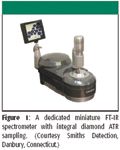
Figure 1
This concept has been taken up by other manufacturers, most notably by SensIR (acquired in 2004 by Smith's Detection, Danbury, Connecticut) (43), with other dedicated systems incorporating low-throughput sampling devices: the IR microscope and diamond-attenuated total reflectance (ATR) accessories. Figure 1 shows an integrated FT-IR–diamond ATR spectrometer. SensIR produced a small interferometer matched to these accessories and again obtained performance equal to that of larger instruments. Today, other small interferometers (44) and dedicated FT-IRs are available (45,46). However, outside the laboratory, small interferometers have been used for decades in dedicated remote sensing applications, going back to the Block Engineering (Marlborough, Massachusetts) model 196 (47); a current example is the D&P Instruments (Simsbury, Connecticut) (48) MicroFT (Figure 2) (49). This employs a pair of potassium bromide sliding prisms, and the higher refractive index of that material enables a larger solid angle to be accepted into the interferometer (and therefore greater throughput), as compared to a mirror-based Michelson design of the same size. This is an example of a field-widened interferometer (50), and a similar approach can be taken in a grating instrument (see below).
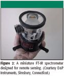
Figure 2
MEMS Fourier-Transform Spectrometers
There are several papers in the literature describing MEMS FT-IR spectrometers, but to the best of the author's knowledge, these have not yet resulted in MIR commercial products from a major or traditional vendor, although two research-company spinoff products are available (see the following). In 1999, Collins and colleagues (51) reported on a miniature, microfabricated spectrometer. This used dovetail microjoints etched from silicon for the bearing of the moving mirror. Although this device was configured for the NIR, it did incorporate a large mirror displacement, providing an optical resolution that was unusually high for a miniature device. The bearing travel was as long as 8 cm, and the measured halfwidth of a laser line was 1 nm. This bearing design has been used to construct a brassboard system for Earth atmospheric studies (37), weighing only 0.5 kg but with a resolution of 0.1 cm–1 . Knipp and colleagues (52,53) described the concept of a standing wave Fourier spectrometer for the visible region, a device that combines aspects of both a traditional Fourier spectrometer and Fabry-Pérot spectrometers. A miniaturized LIGA Fourier-transform spectrometer was described by Solf and colleagues (33), who reported spectra for laser emission and a bandpass filter in the NIR.
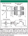
Figure 3
Articles from the University of Neuchâtel (Neuchatel, Switzerland) have described a number of miniature spectrometers. In 1999, the authors presented a MOEMS-based miniaturized Fourier-transform spectrometer (Figure 3), 5 mm × 4 mm × 0.5 mm in size, based upon a silicon comb drive (31), with a resolution of ~10 nm in the visible region. The moving mirror was 75 μm × 500 μm and could incorporate a laser reference. The authors comment that the instrument's resolution is good enough for applications such as color sensors. Further details were given in a second article (54). A third article (35) describes a miniature lamellar grating (55) interferometer, again with dimensions of 5 mm × 5 mm (Figure 4). This had a resolution of 70 cm–1 or 2.8 nm at 633 nm, and the emission spectrum of a xenon lamp was measured. The authors stated that the advantage of this technique was that it required neither a beamsplitter (as compared to a Michelson interferometer) nor an array detector (as compared to a spectrograph) for these measurements. A series of commercial instruments are now available based upon this lamellar-grating technology (56), with 30-cm–1 resolution, and operating in the visible to NIR regions 500–2600 nm). Ataman and colleagues have also described a MEMS lamellar grating spectrometer operating in the visible and NIR (57).
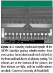
Figure 4
Kraft and colleagues (58–61) have described a number of miniaturized spectrometers, including a spectrometer with a MEMS interferometer. This device employed a resonantly driven micromirror, suspended on two long springs, driven by interlocking comb-structured electrodes (Figure 5), and contained in a vacuum chamber. The effective mirror area was ~1.6 mm2. The first prototype covered a spectral range from ~4500 to 1450 cm–1, using a thermoelectrically cooled MCT detector at a spectral resolution of better than 30 cm–1, and a wavelength stability of better than 4 cm–1. It had a footprint of 180 mm × 120 mm × 120 mm and a mass of about 1.5 kg. This has now been commercialized (62), covering the 2–6 μm range at 30-cm–1 resolution, with 10-cm–1 resolution under development.
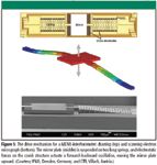
Figure 5
Yu and colleagues (63,64) also described a silicon-MEMS Fourier-transform spectrometer. The silicon beamsplitter, micromirrors, MEMS actuators, and fiber-optic positioners were all fabricated simultaneously by micromachining techniques: they used a combination of deep reactive ion etching and anisotropic wet etching. The footprint of the micromirror assembly was 4 mm × 4 mm. The performance was characterized using an external-cavity tunable laser, and a resolution of about 50 nm was obtained around 1500 nm in the NIR. The authors comment that devices such as this could find application in lab-on-a-chip and optical coherence tomography applications.
Keränen and colleagues (65,66) described a number of miniature spectrometer designs. One MIR spectrometer was composed of three silcon micromachined devices: a pulsed infrared emitter, a tunable Fabry-Pérot interferometer, and a detector. Saari (67) described a second device, a Michelson interferometer that used a series of micromirrors to generate the optical path difference. Five micromirrors are arranged in a two-over-three configuration so that their displacements are additive.
Finally, in 2004, Block Engineering reported (39) on the start of an effort to design, fabricate, and test a MEMS-based FT-IR spectrometer for use in the 2–13.5 μm spectral range (Figure 6). The design described uses an internal source at 800 K and an interferometer with 10-cm–1 resolution coupled to a 1-m White cell. The resolution requires mirror motion on the order of 0.5 mm, which would give a retardation of 1 mm and therefore a spectroscopic resolution of about 10 cm–1. This is in contrast to some of the other designs described earlier, which had mirror displacements around 40–50 μm and resolutions of about 100 cm–1. Block anticipates using a torsional ratchet actuator, converted into linear motion, to achieve this retardation.
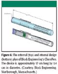
Figure 6
It is clear that for analytical spectroscopy, resolution and throughput are the major issues with these devices. The Block Engineering project has specified a resolution familiar to analytical spectroscopists, but the others are around a factor of ten worse. Throughput remains the largest issue; to overcome this, the data given in most of these papers employs lasers and arc lamps as sources, and not standard analytical transmission samples, let alone diffuse reflectance samples. A typical laboratory FT-IR spectrometer has 30-mm diameter mirrors in the interferometer, giving an area of ~2800 mm2. One of the MEMS-device mirrors noted above had dimensions of 75 μm × 500 μm, giving an area of 0.0375 mm2, a factor of 75,000 less in area. In the best case of operating in the shot-noise limit in the NIR, this implies a factor of ~275 poorer in S/N. The instrument described by Kraft quoted 1.6 mm2, or a factor of 1750 less in area. It is reasonable to assume that it is detector-noise limited, leading to a factor of up to 1750 poorer S/N. As Block Engineering notes in their article, for MIR applications, a MEMS device must have the largest optical component sizes practical. A clear distinction should therefore be made between, on the one hand, the use of MEMS actuators and MEMS fabrication techniques, and on the other hand, the desirable size of the optics.
Other Multiplexing Techniques
We have already noted that Hadamard transform spectrometers are multiplex devices, and therefore can have an advantage in the detector-noise-limited regime (68). Most designs have used linear or rectangular masks, but Harwit and Sloane (69) described a design using a rotating mask with transmitting and reflecting sections (a "0/1" design), and they note some difficulties with this "0/1" implementation. A recent addition to the class of multiplex spectrometers is Aspectrics' (Pleasanton, California) encoded photometric infrared (EP-IR) spectrometer (70,71), and the overall concept and some applications have been described by Coates (6). The optical arrangement is source to sample, to spectrograph with encoder, to single-element detector (Figure 7). This technology can be applied in different spectral regions, but we will consider the MIR version here. Inside the spectrograph, a grating disperses the light from the source and sample onto a rotating encoder disk. This has a series of reflective tracks, each patterned to give a different modulation frequency for the wavelength region falling on it. After reflection, all the reflected light is directed onto a single detector. The tracks on the disk are constructed to give a sinsusoidal, as opposed to "0/1," modulation to the light. A Fourier transform converts the detector signal into a spectrum. The spectrometer has an overall volume of 180 in.3 and weighs 5 lb (4).
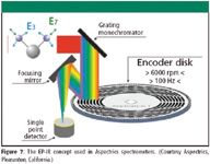
Figure 7
This system therefore bears some resemblances to FT-IR and Hadamard spectrometers, but there are also significant differences. The motion of the modulator is circular and continuous, as opposed to reciprocating, which has both mechanical design and duty cycle advantages. The number of wavelength regions to be examined apparently is limited to 128 currently; the choice of the grating determines the wavelength region to be examined, and the resolution is therefore a function of that range and the number of tracks. As a multiplex technique in a detector-noise-limited regime, this will accrue an advantage, or improvement in S/N, of ~11 (√128), as compared with a scanning grating instrument of the same dimensions and resolution. Unlike an FT-IR spectrometer, this does not have (or does not require) an internal reference laser.
Array Detectors
Visible spectroscopy has profited from the CCD detector, whose technical progress and low cost have been driven by consumer applications, while small NIR spectrometers have been enabled by indium-gallium-arsenide (InGaAs) array detectors, whose rapid development was fueled by the optical telecommunications boom. Unfortunately, there have not been comparable drivers for MIR array detectors, outside the specialist defense arena. Two-dimensional MIR array detectors are expensive; a complete MCT camera can cost in the range of $30,000. Uncooled cameras (72) are somewhat lower cost but are still prohibitive for portable spectrometers. Therefore, the use of array detectors has been largely confined to research-grade spectroscopic imaging systems, which have employed both two-dimensional and linear MCT arrays. However, a very limited number of nonimaging spectrometers with multiplexed linear arrays are available commercially.
Lead sulfide (PbS) arrays cover the range from 1–3 μm, while lead selenide (PbSe) arrays cover from 1–5 μm, and these are available commercially from a number of vendors (73). PbS and PbSe are photon detectors, and uncooled photon detectors perform poorly at wavelengths longer than 5 μm. For that reason, longer wavelength uncooled detectors are thermal devices: bolometers, thermopiles, and pyroelectrics (72). Pyroelectric arrays (74) are available commercially (75), and depending upon the window material employed, these can have coverage to as long a wavelength as 40 μm (250 cm–1). In general, pyroelectric detectors have no dc response; therefore, they require a modulated (chopped or pulsed) infrared source. Microthermopile and microbolometer detectors are still somewhat specialized items, available from a limited number of defense-related companies (3). A monograph by Kruse (71) compares the principal types of uncooled thermal detectors.
Slab-Waveguide Spectrometers
Linear-array detectors have enabled the development of slab waveguide spectrometers, and these are the subject of two review articles that provide design and optical details (3,4). The key concept is that an infrared-transmitting solid medium is used for the body of the spectrograph, filling the space between the entrance slit, grating, and array detector. As compared with a scanning grating spectrometer, this concept has a number of advantages: no moving parts, leading to a simpler, smaller and less massive assembly; a multichannel advantage; and the exclusion of air from the optical path, eliminating absorbances caused by water vapor and carbon dioxide. This concept is therefore attractive for miniature spectrometers. Because a high refractive index material is used as the waveguide, the optical divergence within the spectrograph is reduced, in accordance with Snell's law. Reducing both the focal length and the grating line spacing leads to an overall reduction in the linear dimension of the spectrograph, and optical aberrations also can be reduced. In addition, this design enables a larger optical collection angle for a given resolution: an f/1 beam outside the waveguide becomes an f/2 beam inside. This is akin to field-widening in an interferometer, and it increases the optical throughput and thus the S/N. Finally, this design offers the prospect of a monolithic construction, in which the grating is lithographically constructed onto a face of the waveguide itself.
One of the first spectrometers based upon this concept operated in the visible range and had a polymethylmethacrylate (PMMA) waveguide (76). This was constructed at Oak Ridge National Laboratory (ORNL) (Oak Ridge, Tennessee) using precision machining techniques, which had their origin in defense applications. This technique effectively has been superceded by the semiconductor-based MEMS–MOEMS and LIGA methods described earlier.
Foster-Miller (Waltham, Massachusetts) offers a zinc selenide (ZnSe) slab-waveguide MIR system. ZnSe has a refractive index of about 2.4 in the IR region, allowing a reduced focal length and miniaturization of the device relative to conventional grating systems. The wedged waveguide (Figure 8) is designed to reduce astigmatism in the spectrograph (77,78). This uses a grating bonded to the waveguide with an index-matching glass, and an uncooled, 64-pixel, thermocouple array directly coupled to the waveguide. This system has been adapted for the analysis of used lubricating oils as well as point and standoff chemical–biological sensing (78). An entire handheld, battery-powered device has dimensions of approximately 6 in. × 8 in. × 2 in. and weighs 3.5 lb. Typical analysis times are about 1 min.
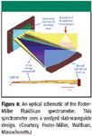
Figure 8
Ion Optics (now ICx Photonics, Billerica, Massachusetts) described a slab waveguide spectrograph design, using either silicon (Si, refractive index ~ 3.4) or germanium (Ge, refractive index ~ 4.0) (2,79). The Si-based spectrograph operated in the 3–5 μm range, with a spectral resolution of 14.5 cm–1, and the Ge-based version operated in the 7–12 μm range, with a resolution of 8 cm–1. In this case, the grating was lithographically constructed on the waveguides. Both systems used a 1 × 64 thermopile array (Bi-Te, Bi-Sb-Te). The use of higher refractive index materials (Si, Ge, as compared with ZnSe) resulted in a smaller spectrograph, 3 in. × 4 in. × 1 in.
Kruzelecky (4,80) has described another variant of this concept. The integrated optical spectrometer (81) has a monolithic design, using either Si or ZnSe waveguides, with the grating formed on the slab waveguide in a multistep lithographic process; it can use either 256-element PbSe or PbS arrays, covering 3–5 μm or 1.1–3.1 μm, respectively. The spectrograph itself can be as small as 3 cm × 4.5 cm, and the complete spectrometer is about 19.5 mm × 19.5 mm × 14 mm, with a mass of less than 2 kg.
Linear Variable Filter Spectrometers
Wilks Enterprise (South Norwalk, Connecticut) offers a compact MIR spectrometer employing a linear variable filter and an uncooled 64-element pyroelectric array, giving a resolution of 40 cm–1, although it can be configured to cover different spectral regions (82,83). This instrument has a built-in ATR sample interface, is 5 in. × 5 in. × 1.5 in., and is targeted at a limited number of liquid-phase industrial applications (Figure 9). Linear variable filters are optical bandpass filters that have been "wedged" in one direction; that is, the thickness of the coatings is not constant across the filter. The transmitted wavelength (or more accurately, the center wavelength of the band transmitted at a point) varies linearly across the filter. The typical range is one octave: if the lowest wavelength is λ, then the highest wavelength is 2λ, and the resolving power is typically 1%. So at a wavelength of λ, the resolution is λ/100; translating that into MIR terms, a typical resolution at 1500 cm–1 would be around 15 cm–1 . The Wilks spectrometer also has a monolithic, no-moving-parts design, with very little free-space light propagation. A 64-element pyroelectric array is also incorporated in an instrument from Artifex Engineering (Emden, Germany) (84). This instrument has a spectral range from 1.5 to 13.5 μm, and the complete optical head has dimensions of 300 mm × 400 mm × 190 mm. The company states that it has applications in the measurement of thin films via emissivity.

Figure 9
Photonic Devices
Photonic crystals (85,86) are another class of devices that were developed during the 1990s (87) and are now beginning to see applications in spectroscopy (88). A photonic crystal consists of a dielectric material (for example, silicon) with a periodic structure, and this creates a bandgap in the material, drastically altering its emission and absorption properties (Figure 10). Optical waves interact with a periodic structure having around the same spatial frequency, leading to bands where light cannot propagate through that medium. This concept has been converted into commercial devices by ICx Photonics (89–91), who developed a MEMS photonic crystal device "tuned" for carbon dioxide detection (Figure 11). The device is less than 0.5-in. square and has a mass of about 5 g. It can detect carbon dioxide in a range of 0–100% with a sensitivity of about 100 ppm. Another device uses a photonic crystal structure to broadly select (that is, confine emission to between 3 and 5 μm) and direct infrared emission in either continuous or pulsed modes. These are not classical blackbody emitters (12), and they can be much more energy efficient, lending themselves to use in many small and portable devices. They may find application in areas in which traditional nondispersive instruments are used today and in air quality and automotive applications.
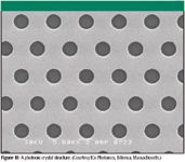
Figure 10
Most MIR spectrometers employ modulated sources of some kind (92), such as a chopper in a classic grating spectrometer or the interferometer in an FT-IR, in order to overcome drift, and they generate an ac signal in a frequency interval that is appropriate for the detector and far away from the largest noise sources in the system. In a miniature MIR "sensor" or spectrograph, the size, energy consumption, and reliability of a mechanical chopper might not be practical, and pulsed sources become practical alternatives. Photonic pulsed sources have an obvious application here.
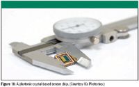
Figure 11
Tunable Lasers
The final approach to fabricating a miniature spectrometer and overcoming the throughput problem is to use a very bright source. Until recently, the only possible solution was to use a synchrotron (93), which hardly makes a portable device. MIR tunable lasers, based upon lead-salt technology, have been available for many years (94), but these were very high resolution (~0.01 cm–1 ), very narrow tuning range (<1 cm–1 ) devices, suitable for gases only. Quantum cascade lasers (95,96) (Figure 12) were developed in the 1990s and became commercially available (97–99) from at least two companies (100,101) recently. The technology behind these devices is described in the literature (95) and will not be summarized here. One commercial laser module is 65 mm × 30 mm × 65 mm with a mass of 300 g, and another is 5.5 in. × 3.45 in. × 3.31 in., but they both require other external electronics and a sampling accessory. These devices have been used for a variety of gas sensing applications (102–105). However, they are not continuously tunable across the MIR; typically, an individual laser can tune ±5% around its center wavelength. For instance, a laser operating at 8 μm (1250 cm–1 ) could therefore tune ±75 cm–1, or from 1175 to 1325 cm–1 . One company states that center wavelengths of 4.5 μm, 4.9 μm, 5.3 μm, 6.2 μm, 8.4 μm, 10.4 μm, and 10.5 μm are available (101). From the examples in the literature, it appears that at the present time, the most promising applications are analysis of complex gas mixtures and fugitive gas emissions. One example shows that many gases absorb in a comparatively narrow range (methane, nitrous oxide, water, and so forth).
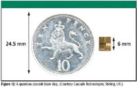
Figure 12
Conclusions
MIR instruments can be miniaturized to a certain extent by shrinking a conventional FT-IR design, especially if care is taken in the choices of sampling accessories and matching their throughput. MEMS FT-IR designs have been executed, principally in the interferometer, but the performance of these devices in the MIR is unproven, especially for traditional analytical applications. Uncooled linear MIR arrays are available and have been used with grating and filter instruments in dedicated applications, while photonic crystals and quantum cascade lasers are finding promising niches in gas detection applications. Multiplex spectrometers using Hadamard techniques are experiencing a renaissance enabled by recent technology, and they are worth considering if other high-throughput and/or multiplex techniques (for example, Mertz's "mock interferometer" [106]) find MEMS implementations. The Fourier and Hadamard implementations might not take full advantage of their multiplex and throughput abilities, but they might have a cost and size advantage by enabling the use of single-element detectors rather than costly MIR arrays.
In many of the instruments described here, a key component has been miniaturized but the remainder of the system (ancillary optics, sample interface, electronics, and user interface) are conventional in design and execution. The greatest gains will be obtained in a systems approach, where every component is optimized and miniaturized.
Other technologies developed during the telecommunications boom have their greatest impact in the NIR region, which will be described in the second article in this series.
Acknowledgments
The author thanks the following individuals and companies for permission to reproduce the figures: John Seelenbinder (Smiths Detection), Win Wadsworth (D&P Instruments), Hans Peter Herzig (University of Neuchâtel), Omar Manzardo (ARCoptix), Harald Schenk (IPMS, Dresden), Martin Kraft (CTR), Petros Kotidis (Block Engineering), Bob Messerschmidt (Aspectrics), Mitch Shikowitz (Foster-Miller), Paul Wilks (Wilks Enterprise), Ed Johnson (ICx Photonics), and Yann Hamonou (Cascade Technologies).
Richard A. Crocombe is with ThermoFisher Scientific in Billerica, Massachusetts.
References
(1) J.P. Smith, Anal. Chem. 72, 653A–658A (2000).
(2) C.M. Harris, Anal. Chem. 75, 75A–78A (2005).
(3) J.T. Daly, E.A. Johnson, A. Bodkin, W.A. Stevenson, and D.A. White, Proc. SPIE 3953, 70–87 (2000).
(4) R.V. Kruzelecky and A.K. Ghosh, "Miniature Spectromers," in The Handbook of Vibrational Spectroscopy, Vol. 1 (John Wiley & Sons, Ltd., New York, 2002).
(5) J.P. Coates, Spectroscopy 15(12), 21–27 (2000).
(6) J. Coates, Spectroscopy 20(1), 32–41 (2005).
(7) J. Coates, Spectroscopy 21(2), 68–74 (2006).
(8) J. Coates, Spectroscopy 21(10), 20–25 (2006).
(9) J. Coates, Spectroscopy 22(2), 28–38 (2007).
(10) C.M. Christenson, The Innovator's Dilemma: When New Technologies Cause Great Firms to Fail (Harvard Business School Press, Boston, 1997).
(11) R.P. Feynman, "Plenty of Room at the Bottom," California Institute of Technology, December 1959. www.its.caltech.edu/~feynman/plenty.html.
(12) G.W. Chantry, Long Wave Optics (Academic Press, New York, 1984), p. 337.
(13) P.R. Griffiths and J.A. de Haseth, Fourier Transform Infrared Spectrometry (John Wiley & Sons, New York, 1986), Chapter 7.
(14) R.L. McCreery, Raman Spectroscopy for Chemical Analysis (John Wiley & Sons, New York, 2000), Chapter 4.
(15) G.W. Chantry, Long Wave Optics (Academic Press, New York, 1984), pp. 76, 542.
(16) M. Harwit and N.J.A. Sloane, Hadamard Transform Optics (Academic Press, New York, 1979), p.3.
(17) Robert John Bell, Introductory Fourier Transform Spectroscopy (Academic Press, New York, 1972), pp. 19–25.
(18) M. Harwit, "Hadamard Transform Analytical Systems," in Transform Techniques in Chemistry, Peter R. Griffiths, Ed. (Plenum Press, New York, 1978), Chapter 7; J.A. Decker, Jr., "Hadamard Transform Spectroscopy," in Spectrometric Techniques, George A. Vanesse, Ed. (Academic Press, New York, 1977), Chapter 5; M. Harwit and N.J.A. Sloane, Hadamard Transform Optics, (Academic Press, New York, 1979).
(19) M. Wippich and K.L. Dessau, The Industrial Physicist 24–27 (June/July 2003).
(20) B.E. A Saleh and M.C. Teich, Fundamentals of Photonics, 2nd edition, (Wiley-Interscience, Hoboken, 2007).
(21) M.Gad-el-Hak, Ed., The MEMS Handbook, 2nd ed. (CRC Press (Taylor & Francis, New York), 2005).
(22) J. Rasmussen and J. Krafcik, Small Times 7(4), 24–25 (July/August 2004).
(23) R&D Magazine, pp. 33–37 (July 2007), downloadable at www.rdmag.com/pdf/RD0707_Materials.pdf.
(24) www.wtc-consult.de/english/pr102.html.
(25) H. Weinberg, Sensors, February 2002, www.archives.sensorsmag.com/articles/0202/36/index.htm.
(26) www.dlp.com/tech/what.aspx.
(27) J.S. Niew, Wireless Design & Development 4, 30–31 (2002).
(28) S.F. Gale, Small Times, (January 2007), www.smalltimes.com/display_article/281842/109/ARTCL/none/none/1/MEMS-the-word-in-consumer-electronics/.
(29) R. Allan, Small Times7(4), 18–20 (July 2007).
(30) R.F. Wolffenbuttel, IEEE Trans. Instrum. Meas. 53, 197–202 (2004).
(31) P.C. Montgomery, D. Montaner, O. Manzardo, M. Flury, and H.P. Herzig, Thin Solid Films450, 79–83 (2004).
(32) J. Antoszewski, J. Dell, T. Shivakumar, M. Martyniuk, K. Winchester, J. Wehner, C. Musca, and L. Faraone, Proc. Soc. Photoinst. Opt. Eng. 4935, 148–155 (2002).
(33) C. Solf, J. Mohr and U. Wallrabe, Sensors 2003, Proceedings of IEEE 2, 773–776 (2003).
(34) A. Barwicz, IEEE Instrumentation & Measurement Magazine 7(2), 14–19, (June 2004).
(35) O. Manzardo, H.P. Herzig, C.R. Marxer, and N.F. de Roonij, Opt. Lett. 24, 1705–1707 (1999).
(36) O. Manzardo, R. Michaely, F. Schädelin, W. Noell, T. Overstolz, N. de Rooij, and H.P. Herzig, Opt. Lett. 29, 1437–1439 (2004).
(37) G. Jodor, M. Sirota, H. Riris, W. Hasselbrack, Fourier Transform Spectroscopy, Optical Society of America Trends in Optics and Photonics 84, 55–58 (2003).
(38) P. Krippner, T. Kuehner, J. Mohr, and V. Saile, Proc. SPIE 3912, 141–149 (2000).
(39) E.R. Schildkraut, D. Reyes, D.J. Cavicchio, and J.O. Jensen, "A MEMS Based Micro-Spectrometer For Toxic Vapor Detection And Identification", Presented at the Scientific Conference on Chemical and Biological Defense Research (2004) held in Hunt Valley, Maryland, on 15–17 November 2004. Available on Block Engineering web site: www.blockeng.com/huntvalley.pdf.
(40) J.A. Mohr, A. Last, U. Hollenbach, T. Oka, and U. Wallrabe, Journal of Lightwave Technology 21, 643–647 (2003).
(41) D. Brennan, J. Alderman, L. Sattler, B. O'Connor, and C. O'Mathuna, Measurement 33, 67–74 (2003).
(42) F. Gindele and C. Novotny, Proc SPIE 4943, 47–58 (2003).
(43) Now Smiths Detection (Danbury, Connecticut).
(44) Noveltech Solutions Ltd. (Turku, Finland), www.noveltechsolutions.com.
(45) R. Mukhopadhyay, Anal. Chem. 76, 169A–372A (2004).
(46) In addition, A2 Technologies (Danbury, Connecticut) and Bruker Optics (Billerica, Massachusetts) both introduced small FT-IR spectrometers at the 2007 Pittsburgh Conference.
(47) P.R. Griffiths, Chemical Infrared Fourier Transform Spectroscopy (John Wiley, New York, 1975), pp 99–100.
(48) D&P Instruments (Simsbury, Connecticut), www.dpinstruments.com/.
(49) A.R. Korb, P. Dybwad, W. Wadsworth, and J.W. Salisbury, Appl. Opt. 35, 1679–1692 (1996).
(50) D. Baker, Chapter 2 in Spectrometric Techniques, George A. Vanesse, Ed. (Academic Press, New York, 1977).
(51) S.D. Collins, R.L. Smith, C. González, K.P. Stewart, J.G. Hagopian, and J.M. Sirota, Opt. Lett. 24, 844–846 (1999).
(52) D. Knipp, H. Stiebig, S.H. Bhalotra, H.L. Kung, and D.A.B. Miller, MOEMS and Miniaturized Systems III, Proc. SPIE 4983,127–138 (2003).
(53) D. Knipp, H. Stiebig, S.H. Bhalotra, H.L. Kung, and D.A.B. Miller, IEEE Trans. Electron Devices, 52, 419–426 (2005).
(54) P.C. Montgomery, D. Montaner, O. Manzardo, M. Flury, and H.P. Herzig, Thin Solid Films 450, 79–83 (2004).
(55) S.F. Johnston, Fourier Transform Infrared: A Constantly Evolving Technology (Ellis Horwood, West Sussex, UK, 1991), pp. 192–197; R.J. Bell, Introductory Fourier Transform Spectroscopy (Academic Press, New York, 1972), pp. 200–230.
(56) ARCOPTIX S.A. (NeuchE2tel, Switzerland), www.arcoptix.com.
(57) C. Ataman, H. Urey, S.O. Isikman, and A. Wolter, Proc. SPIE 6186, C1–C9 (2006).
(58) M. Kraft, A. Kenda, and H. Schenk, "Hand-held high-speed spectrometers based upon Micro-Electro-Mechanical components", Proceedings of the Symposium on Photonics Technologies for the 7th Framework Program, Wroclaw, 183–186 (October 2006).
(59) M. Kraft, "Compact MEMS High-Speed Fourier-Transform Spectrometer," presented at the 4th International Conference on Advanced Vibrational Spectroscopy, Corfu, June 2007: www.icavs.info/downloads/corfu2007/contributed/Martin_Kraft.pdf.
(60) T. Sander, A. Kenda, C. Drabe, H. Schenk, and W. Scherf, Proc. SPIE 6466, 1–12, (2007).
(61) A. Kenda, C. Drabe, H. Schenk, A. Frank, M. Lenzhofer, and W. Scherf, Proc. SPIE 6186, 1–11, (2006).
(62) Carinthian Tech Research AG (Villach, Austria); www.ctr.at.
(63) K. Yu, D. Lee, U. Krishnamoorthy, N. Park, and O. Solgaard, Sensors and Actuators A 130–131, 523–530 (2006).
(64) K. Yu, N. Park, D. Lee, and O. Solgaard, IEEE Sensors 2006, EXCO, 412–415 (October 2006).
(65) K. Keränen, M. Blomberg, O. Rusanen, P. Karioja, J. Tenhunen, and H. Kopola, Proc. SPIE 3631, 165–172 (1999).
(66) K. Keränen, P. Karioja, M. Blomberg, J. Tenhunen, O. Rusanen, and H. Kopola, SPIE Opt. Eng. 40(10), 2308–2314 (2001).
(67) H. Saari, "Optical Microsensors" in Microsensing Spring 2001: www.fyslab.tkk.fi/kurssit/Tfy-3.480/Spring2006/0215-Saari/luennot.pdf.
(68) J.A. Decker, Jr., "Hadamard Transform Spectroscopy," in Spectrometric Techniques; G.A. Vanesse, Ed. (Academic Press, New York, 1977).
(69) M. Harwit and N.J.A. Sloane, Hadamard Transform Optics (Academic Press, New York, 1979), pp. 31, 167–172.
(70) Aspectrics (Pleasanton, California), www.aspectrics.com.
(71) US Patent 6,999,165, Hagler, "Method and apparatus for radiation analysis and encoder," and references to other patents therein.
(72) P.W. Kruse, Uncooled Thermal Imaging: Arrays, Systems and Applications (SPIE Press, Bellingham, Washington, 2001).
(73) Cal Sensors (Santa Rosa, California), New England Photoconductor (Norton, Massachusetts), Northrop Grumman (Tempe, Arizona), SensArray Infrared (Burlington, Massachusetts).
(74) P. Muralt, Rep. Prog. Phys. 64 1339–1388 (2001); R. Passerini, M. Kohli, P. Ryser, A. Seifert, B. Willing, and P.-Y. Cattin, Proc. SPIE 5251, 89–96 (2004).
(75) Irmicrosystems (Lausanne, Switzerland), www.ir-microsystems.com/web/products/microray.php.
(76) S. Rajic, C.M. Egert, B.M. Evans III, J.P. Cunningham, and T.A. Marlar, Proc. SPIE 2536, 452–462 (1995).
(77) S. Chadha, W. Kyle, R. Bolduc, and L.A. Curtiss, Proc. SPIE 3859, 130–135 (1999); US Patent 5,856,870, Curtiss, "Spectroanalytical System." See also FluidScan-H: www.foster-miller.com/handheld_oil_monitor.htm.
(78) S. Chadha, C. Stevenson, and L.E. Curtiss, Proc. SPIE 3533, 103–113 (1999); S. Chadha, P. Henning, F. Landers, and A. Weling, Proc. SPIE 5269, 42–54 (2004).
(79) US Patent 6,303,934, Daly, Bodkin, Groden, and Johnson, "Monolithic infrared spectrometer apparatus and methods."
(80) R.V. Kruzelecky, S. Paquet and A.K. Ghosh, Proc. SPIE 2744, 684–695 (1996); R.V. Kruzelecky, A.K. Ghosh, C. Tremblay, and C. Paquet, Proc. SPIE 3416, 13–22 (1998); R.V. Kruzelecky and A.K. Ghosh, Proc. SPIE 4205, 25–34 (2001); US Patent 7,034,935, Kruzelecky, "High performance miniature spectrometer."
(81) MPB Technologies, Pointe Claire, Quebec, Ontario, Canada, www.mpb-technologies.ca/mpbt/Space/pages/mpb-photonics-devices.html.
(82) Wilks Enterprise, Inc., South Norwalk, Connecticut, www.wilksir.com/vfa-spectrometer.htm.
(83) P. Wilks, "Infrared Filtrometers," in The Handbook of Vibrational Spectroscopy, Volume 1 (John Wiley & Sons Ltd., New York, 2002).
(84) Artifex Engineering (Emden, Germany), www.artifex-engineering.com.
(85) J. Hecht, Laser Focus World (March 2005), www.laserfocusworld.com/display_article/224011/12/ARCHI/none/Feat/Photonic-crystals-offer-a-host-of-possibilities.
(86) B.E.A Saleh and M.C. Teich, Fundamentals of Photonics, 2nd ed. (Wiley-Interscience, Hoboken, 2007), Chapter 7.
(87) J. Ouelette, The Industrial Physicist, 14–17 (December 2001/January 2002).
(88) I. Puscasu, SPIE OE Magazine, 21–23 (May 2003).
(89) Now ICx Photonics (Billerica, Massachusetts), www.icx-photonics.com/ICX-Photonics.asp.
(90) J. Mallozzi, R&D Magazine, 22 (Oct. 2005), www.rdmag.com/pdf/ONE/0510BreakthroughIREmitters.pdf
(91) I. Puscasu, M. Pralle, M. McNeal, A. Greenwald, Ed Johnson, and A.A. Shah, "Photolithographically controlled emission from photonic crystals" in "Nanosensing: Materials and Devices II," M.S. Islam and A.K. Dutta, Eds., Proc. SPIE 6008, 0Y-1 (2005).
(92) G.W. Chantry, Long Wave Optics (Academic Press, New York, 1984), p. 294.
(93) G.L. Carr, J. Reffner, and G.P. Williams, Rev. Sci. Instr. 66, 1490 (1995).
(94) H.R. Schlossberg and P.L. Kelley, in Spectrometric Techniques, Volume 2, George A. Vanesse, Ed. (Academic Press, New York, 1981), Chapter 4.
(95) B.E.A. Saleh and M.C. Teich, Fundamentals of Photonics, 2nd ed. (Wiley-Interscience, Hoboken, 2007), Chapter 17.
(96) J. Faist, Optics and Photonics News, 32–36 (May 2006).
(97) Alpes Lasers (Neuchâtel, Switzerland), www.alpeslasers.ch/.
(98) J. Ouelette, The Industrial Physicist, 8–13 (April/May 2001).
(99) I. Howieson, E. Normand, and M.T. McCulloch, Laser Focus World (March 2005), www.laserfocusworld.com/display_article/224013/12/ARCHI/none/OptWr/Quantum-cascade-lasers-smell-success.
(100) Cascade Technologies (Stirling, Scotland), www.cascade-technologies.com
(101) Daylight Solutions (Poway, California), www.daylightsolutions.net.
(102) M.T. McCulloch, N. Langford, and G. Duxbury, Appl. Opt. 44, 14 (2005).
(103) M. Garcia, E. Normand, C.R. Stanley, C.N. Ironside, C.D. Farmer, G. Duxbury, and N. Langford, Opt. Commun. 226, 39 (2003).
(104) M.J. Weida, D. Arnone, and T. Day, Laser Focus World (July 2006), www.laserfocusworld.com/display_article/259939/12/none/none/OptWr/Tunable-QC-laser-opens-up-mid-IR-sensing-applications.
(105) G. Duxbury and N. Langford, Spectroscopy Europe 18(5), 18–22 (2006).
(106) L. Mertz, Transformations in Optics (Wiley, New York, 1965).

AI Shakes Up Spectroscopy as New Tools Reveal the Secret Life of Molecules
April 14th 2025A leading-edge review led by researchers at Oak Ridge National Laboratory and MIT explores how artificial intelligence is revolutionizing the study of molecular vibrations and phonon dynamics. From infrared and Raman spectroscopy to neutron and X-ray scattering, AI is transforming how scientists interpret vibrational spectra and predict material behaviors.
Real-Time Battery Health Tracking Using Fiber-Optic Sensors
April 9th 2025A new study by researchers from Palo Alto Research Center (PARC, a Xerox Company) and LG Chem Power presents a novel method for real-time battery monitoring using embedded fiber-optic sensors. This approach enhances state-of-charge (SOC) and state-of-health (SOH) estimations, potentially improving the efficiency and lifespan of lithium-ion batteries in electric vehicles (xEVs).
New Study Provides Insights into Chiral Smectic Phases
March 31st 2025Researchers from the Institute of Nuclear Physics Polish Academy of Sciences have unveiled new insights into the molecular arrangement of the 7HH6 compound’s smectic phases using X-ray diffraction (XRD) and infrared (IR) spectroscopy.