The Revolution in Energy Dispersive X-Ray Spectrometry: Spectrum Imaging at Output Count Rates Above 1 MHz with the Silicon Drift Detector on a Scanning Electron Microscope
The author discusses the improvements offered by silicon drift detector energy dispersive X-ray spectrometry (SDD-EDS) systems over the classic Si(Li)-EDS for mapping the compositional microstructure of matter with scanning electron microscopy (SEM).

The silicon drift detector energy dispersive X-ray spectrometry (SDD-EDS) system offers revolutionary improvements over the classic Si(Li)-EDS for mapping the compositional microstructure of matter with scanning electron microscopy (SEM). For a given spectral resolution and detector solid active area/solid angle, SDD-EDS provides a throughput, measured as the peak output count rate, that is at least 50 times faster than Si(Li)-EDS. This high throughput directly translates into greatly reduced times for X-ray elemental mapping. Operating in the X-ray spectrum image (XSI) mode in which a complete EDS spectrum is recorded at each beam position, SDD-EDS can capture maps of useful pixel density (256 ‗ 192) in less than 5 s that record information on major and minor constituents. Additional XSI mapping strategies include high pixel density (1024 ‗ 768) and high intensity range for more complete recording of minor and trace constituents. Combined with the high brightness, high beam current, thermally assisted field emission gun SEM, high spatial resolution approaching 100 nm can be achieved in SEM–SDD-EDS X-ray maps.
Scanning electron microscopy (SEM) combined with energy dispersive X-ray spectrometry (EDS) has become a mainstay of microstructural characterization with many fields of application, from biology to geology to materials science as well as failure analysis (1). The Si(Li) energy-dispersive X-ray spectrometer has more than 40 years of service as an analytical spectrometer for X-rays excited by beams of electrons as well as by primary X-rays in the bulk analysis method of X-ray fluorescence and by ion beams from high-energy accelerators (2). Despite the maturity of Si(Li)-EDS, the energy-dispersive spectrometry field is undergoing a profound change due to the recent emergence of the silicon drift detector (SDD) (3). Photon detection with semiconductor EDS involves the photoelectric absorption of the X-ray photon and ejection of the energetic photoelectron within the active semiconductor volume. Subsequent inelastic scattering of the energetic photoelectron (and any Auger electrons emitted during the de-excitation of the Si ionization state) results in the creation of electron-hole pairs in numbers proportional to the original energy of the X-ray. A transverse potential field imposed across the thickness of the Si by uniform electrodes on the entrance and back surfaces separates the free electrons and holes, and the charge collected is proportional to the original photon energy. For the SDD-EDS system, as shown in Figure 1, the same charge-generation process operates, but the SDD-EDS system collects the charge in a markedly different way from the Si(Li)-EDS system. The SDD-EDS system is much thinner, 300 μm to 450 μm compared with 3 mm for the Si(Li)-EDS system, so the transverse distance the charge must travel is reduced by as much as an order of magnitude. A strong radial collection field is created in the SDD-EDS system by the pattern of discrete, nested, back surface electrodes (rings or hexagons). The pattern of potential imposed on these discrete electrodes creates a radial as well as a transverse electrical field that produces a "collection channel," which collects and directs the free electrons to the small central anode, which is about 80 μm in diameter. For a 50 mm2 active detector area, the SDD-EDS system's anode is approximately 10,000 times smaller than the anode of the Si(Li)-EDS system. Because a major contribution to the noise budget of any semiconductor EDS system is related to the area of the anode, for the SDD-EDS system, this noise term is reduced greatly compared with the Si(Li)- EDS system. The SDD-EDS design enables performance that is equal to or substantially better than the Si(Li)-EDS system in the following aspects (4):

Figure 1: Schematic showing the important features of the silicon drift detector EDS system.
• Due to the greatly reduced anode noise contribution, the SDD-EDS system can operate at –25 °C, which can be obtained readily with Peltier electronic cooling exhausted to a heat pipe with external passive radiators compared with the Si(Li)-EDS system, which requires liquid nitrogen cooling to –190 °C. This simplifies the accommodation of the SDD-EDS system into complex electron microscopes as well as other analytical hardware.
• For a given active area, resolution of the SDD-EDS system is better. For example, 122.5 eV (measured as the full peak width at half peak maximum intensity at MnKα, 5890 eV) for a 10-mm2 detector area compared with 129 eV for Si(Li). The superior SDD resolution performance is obtained for low energy photons below 1 keV, as seen in Figure 2. The BeK peak is well separated from the low energy noise peak.
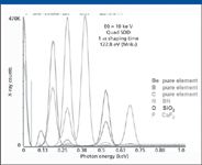
Figure 2: SDD-EDS performance for low-energy photons.
• SDD-EDS peak resolution and peak position are extremely stable over the full range of deadtime, with the SDD-EDS performance illustrated in Figure 3, where the MnKα-MnKβ peaks (scaled to a common peak integral) overlap over an input count rate from 8 kHz to 800 kHz.

Figure 3: Overlap of MnKα - MnKβ peaks (scaled to the same integral) for eight different input count rates ranging from 8 kHz to 800 kHz.
• SDD-EDS achieves a given resolution with a much shorter amplifier time constant than Si(Li)-EDS. Thus, for a 10-mm2 active area, SDD-EDS achieves a resolution of 127.5 eV with an amplifier time constant of 470 ns, whereas a resolution of 129 eV with Si(Li)-EDS typically requires an amplifier time constant of 50 μs.
• As a result of item 4, for a given resolution and active area, the maximum throughput of the SDD-EDS system is at least 60 times faster. For example, Si(Li)-EDS at 129 eV resolution gives a peak in the output count rate (OCR) versus input count rate (ICR) curve of 2 kHz, while SDD-EDS reaches 130 kHz (at 127.5 eV resolution). It is worth noting that, due to limitations of existing digital pulse processing systems, at high deadtime SDD-EDS spectra are subject to significant pulse coincidence, leading to "pile-up peaks" as well as pile-up distortions to the background. Research is currently being performed by the detector community into advanced methods of high-speed pulse processing to correct this problem.
• Clusters of SDDs can achieve throughput 200 times greater than Si(Li)-EDS for the same resolution. Figure 4 shows the OCR versus ICR performance of a cluster of four 10-mm2 SDD-EDS detectors operating with combined output at three different time constants. The dotted line shows the performance of an "ideal" EDS detector with no deadtime, so that OCR = ICR. The deviation of the measured OCR versus ICR curves from the ideal curve is a result of the deadtime associated with the processing of pulses. Only one pulse can be processed at a time, and if a second photon enters the detector while the detector is "busy," inspection circuitry discards this second pulse. If the measurement of the first pulse is considered compromised by the arrival of the second, it too is discarded, leading to the reduction in OCR compared to ICR and an eventual peak in the OCR. At the shortest time constant of 220 ns, the peak of the OCR versus ICR curve exceeds 1 MHz.

Figure 4: Output count rate (OCR) versus input count rate (ICR) for three amplifer time constants: 220 ns, 470 ns, and 1000 ns for a Bruker Quad SDD-EDS system (four 10-mm2 detectors) achieving the indicated resolution at MnKα. Estimated error bars are smaller than the plotting symbols.
In only one major operational parameter does Si(Li)-EDS outperform SDD-EDS. Because of the reduced thickness, 0.3 to 0.45 mm thick for the SDD-EDS system compared with the 3-mm-thick Si(Li)-EDS system, the efficiency for high-energy photons above 10 keV is reduced for SDD-EDS compared with Si(Li)-EDS. For example, Si(Li)-EDS is 100% efficient for U Lα at 13.61 keV compared with the SDD-EDS (0.45 mm) efficiency of 70%, and above a photon energy of 25 keV, the efficiency of SDD-EDS decreases to only a few percent.
X-Ray Mapping Strategy with SDD-EDS
Instrumentation
Elemental mapping with EDS in the scanning electron microscope has been one of the most popular and powerful information output modes throughout the 40-year history of Si(Li)-EDS. Operation in the mapping mode inevitably reduces the X-ray counts accumulated at each beam location on the specimen compared with conventional single point analysis by the the total number of picture elements (pixels), given by the product x-dimension * y-dimension of the scan. Because of the relatively long amplifier time constant of Si(Li)-EDS, elemental mapping has always required several concessions by the analyst.
Operation with reduced spectral resolution to obtain a greater throughput: If the characteristic X-ray peaks are sufficiently separated that peak overlap does not occur, then a higher output count rate can be obtained at the expense of poorer spectral resolution. For a particular 30-mm2 Si(Li)-EDS system of recent manufacture, optimum resolution of 134 eV (FWHM at MnKα) required a time constant of 50 μs, resulting in a peak of 1900 c/s in the OCR versus ICR function, while a time constant of 4 μs raised the OCR maximum to 22.5 kHZ but with a degradation of resolution to 178 eV.
Long accumulation time: Even with the resolution compromise, many minutes to several hours are required to accumulate a map of 256 × 256 pixels with a sufficient intensity range to render an eight-bit gray scale sensitive to major and minor constituents, where these terms are given the following arbitrary definitions:
major: concentration (C) > 0.1 mass fraction
minor: 0.01 < C < 0.1
trace: C < 0.01
Reduced pixel density compared with SEM images: SEM images with secondary electron (SE) and backscattered electron (BSE) signals typically are recorded with pixel density of 512 × 512 or 1024 × 1024. The reduced pixel density of the X-ray maps requires processing of the SEM image to adjust the pixel density downward for matching.
The extraordinary OCR versus ICR throughput capability of SDD-EDS, shown in Figure 4, can have a tremendous impact on all aspects of analytical X-ray spectrometry, and in particular upon X-ray elemental mapping. To achieve the maximum improvement, the measurement must be optimized in several aspects.
To take advantage of the throughput capability of SDD-EDS, the intensity of the X-ray source at the specimen must be increased compared with the conventional operating conditions used for Si(Li)-EDS. All SEM signals, including characteristic X-rays, increase linearly with the beam current that strikes the specimen. For the same detector solid angle for Si(Li)-EDS and SDD-EDS, which is given by the detector active area divided by the square of the distance to the X-ray source, a much higher beam current (100 nA or more) must be supplied to create the high count rates for SDD-EDS shown in Figure 4, compared with the typical values (1 nA or less) required to saturate the response of Si(Li)-EDS at the same resolution.
Fortunately, the development of SEM in recent years has led to the emergence of the thermally assisted field-emission gun source (tFEG) (1). The tFEG-SEM system is capable of both high brightness and high total current, delivering a highly stable beam current into a small probe (for example, 10 nA into a 4-nm probe and 100 nA into a 40-nm probe). Examples of the SEM–BSE image resolution that beams with currents in this range permit are shown in Figure 5. X-ray mapping with SDD-EDS can thus be complemented with high-resolution SEM imaging with the secondary electron and backscattered electron signals. As shown in the following sections, this enhanced spatial resolution performance can be realized even in the elemental maps derived from X-ray spectrum image (XSI) mapping.
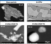
Figure 5: SEM (backscattered electron signal) images of various materials at the indicated beam current.
The solid angle of the SDD-EDS system can be maximized by placing a detector with as large an active area as possible at the minimum possible distance to the source of X-rays at the specimen. Fortunately, large area SDD-EDS detectors are available, with active areas as large as 80 mm2. Because the cooling requirements of SDD-EDS are much more modest than for Si(Li)-EDS, the SDD-EDS system can be placed close to the specimen. An SDD detector of 80 mm2 area A, at a distance s, of 10 mm provides a solid angle Ω = A/s2 of 0.8 steradian, or a geometric efficiency of 12.7% of the unit hemisphere (2π steradians) of total X-ray emission from a thick specimen. This aspect of SDD-EDS remains to be fully exploited, and designs to increase the solid angle of collection involving up to four discrete circumferential detectors with ganged output or a single annular detector have been demonstrated (5).
The X-ray pulse stream produced by the SDD-EDS with a short amplifier time constant demands special processing methods to avoid losing the throughput advantage elsewhere in the signal chain. "Event streaming" methods that utilize fast specialized hardware processing rather than slower software processing have operated successfully with the highest SDD-EDS throughput rates demonstrated (6).
To maximize efficiency, the data collection strategy is to record the entire X-ray spectrum at each pixel, creating an "X-ray spectrum image" (XSI) (7). This powerful data collection method, which is well established in commercial software systems for Si(Li)-EDS, in principle captures all possible elemental composition information about the mapped area within the limitations imposed by the EDS detector performance, the details of the X-ray production and emission, and the dose (beam current and pixel dwell time). By exploiting the high throughput of SDD-EDS, the resulting XSI databases can be populated with much greater numbers of X-ray counts compared with Si(Li)-EDS for the same amount of clock time.
Data Mining the XSI
The XSI can be thought of in two different ways, illustrated in Figure 6. As recorded during the scan, the XSI is an x-y-n(E) array of discrete SDD-EDS spectra where (x,y) represents a pixel and n(E) is the EDS spectrum stored as the number of counts, n, in a channel of energy E with effective width 5 eV or 10 eV. The number of channels stored is typically 2048 or 4096. Figure 6 also contains an alternative view of the XSI as a stack of individual x-y images, each of which represents an individual photon energy, E. The stack can be thought of as a "deck of cards," and Figure 6 shows the images that result when two cards at different energies are chosen.

Figure 6: Two views of the X-ray spectrum image: as an x-y datacube of EDS spectra and as a stack of images, each of which represents a single photon energy, E.
The analyst's task is to discover the information contained within the XSI, which can be as large as several gigabytes. Different approaches to this "data mining" problem have been presented (8–10). For the examples presented here, the technique of calculating "derived spectra," has been used, which are determined with the NIST Lispix software engine from the array of true spectra that constitutes the XSI datacube (8). Figure 7 shows the method of calculating the SUM derived spectrum, in which all of the X-ray counts on an individual image card (that is, one image from the deck of images) are added, and that single summed value represents that photon energy in the construction of the SUM spectrum (7).
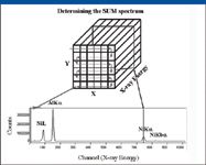
Figure 7: Method for determining the SUM derived spectrum; XSI of Raney nickel.
The SUM spectrum has all of the familiar properties of a measured EDS X-ray spectrum: characteristic peaks, continuum (electron bremsstrahlung) background, and artifacts such as the silicon escape peak and coincidence peaks. Peaks that appear in the SUM spectrum represent prominent compositional features. Raising the vertical display sensitivity (or plotting the log of the SUM) can reveal minor and trace-level peaks, as well as the artifacts. The SUM spectrum is the analyst's guide as to which cards to select from the deck for inspection.
To reduce the effect of the noise arising from the limited counting statistics available at single pixels, a band of energy covering several contiguous cards is defined using the SUM spectrum, and the image retrieval function in NIST Lispix averages the corresponding pixels to produce a final image for display (with the intensity range typically mapped onto the full 8-bit grayscale range of the final display).
While the SUM spectrum is always inspected as the first step in analyzing an XSI database, it is insensitive to statistically rare compositional features that occur at only a few pixels, being overwhelmed by the large number of counts on any card due to the X-ray continuum background. The maximum pixel spectrum, illustrated in Figure 8, provides sensitivity to the "needle in the haystack problem." The maximum pixel spectrum follows the same pathway through the XSI as the SUM spectrum, but instead of adding, it tests each pixel on a card to find the maximum value, which then represents that energy when constructing the maximum pixel-derived spectrum.
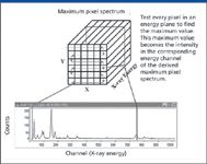
Figure 8: Method for determining the maximum pixel spectrum; same XSI as Figure 7.
An example of the sequential application of derived spectra is shown in Figure 9 for the Raney nickel alloy. The major peaks in the SUM spectrum correspond to the Al and Ni maps, and the minor Fe component is revealed by expansion of the vertical axis. The maximum pixel spectrum shows the presence of an unexpected peak for CaKα (the CaKβ is below detection), and the image constructed from this peak reveals a single pixel, probably as a result of a particle of contamination. Not only does the maximum pixel spectrum aid the analyst in finding the needle in the haystack, the analyst does not even need to know in advance that he is looking for a needle, as in this case, where Ca is not an expected component of the Raney nickel alloy under study.
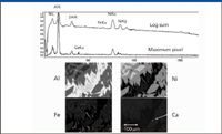
Figure 9: Example of the application of the SUM and maximum pixel derived spectra to reveal major (Al and Ni) and minor (Fe) constituent features as well as an unexpected single pixel feature (Ca).
Examples of Application of tFEG-SEM/SDD-EDS XSI
The overall aim of the examples presented here is to illustrate the extraordinary depth of information that can be captured in a few minutes to a few seconds of real (clock) time. This short time scale, which should be within the patience quotient of most analysts, represents a remarkable time compression compared to the traditional mapping situation with SEM–Si(Li)-EDS.
Achieving Useful Speed: XSI Mapping in 5 s for Heterogeneous Particles
Microscopic particles constitute an important class of materials that SEM-EDS is often called upon to characterize. The typical particle X-ray data collection strategy is either to place a point beam upon the approximate center of the particle or to "overscan" the particle with a scan pattern that either brackets the particle or is confined within the particle image and so collects an "average" EDS spectrum. Both strategies assume the particle is homogeneous, which might not be the case. SDD-EDS XSI mapping can reveal heterogeneous particles directly, as shown in Figure 10 for a particle for which a useful XSI was recorded in less than 5 s. The SUM spectrum reveals the peaks for CuKα and ZnKα, resulting in the images shown, and identifying the overall composition as that of brass. The corresponding SEM-BSE image reveals the localization of a higher average atomic number region, and examination of the SUM spectrum reveals the PbM and PbL peaks, which result in the Pb image shown in Figure 10. The NiKα peak is also found in the expanded SUM spectrum, and the corresponding Ni image shows that it forms a significant and widely distributed component of the particle. Note that the nickel does not produce significant contrast in the SEM-BSE image because of its similar atomic number to the Cu and Zn of the brass. Additionally, the maximum pixel spectrum reveals the unexpected presence of Ti, Fe, and Ca, images of which are shown in Figure 10. Thus, with the investment of 5 s to record an XSI, a much more complete understanding of the particle microstructure is obtained.

Figure 10: Elemental images derived from an XSI (640 à 480 pixels, 16 μs dwell) recorded in 5 s from a complex particle.
Achieving High Pixel Density XSI Mapping
Traditionally, the analyst has had to be satisfied with X-ray maps recorded at pixel densities that are much lower than the densities used for SEM images with SE or BSE signals. Note that this pixel density refers only to the recording of the data and not to the independence of the pixels, which depends upon the size of the pixel relative to the interaction volume, which in turn depends upon the specimen composition, the incident beam energy, and the beam size. Typically, the lateral linear dimensions of the interaction volume for direct electron excitation of X-rays range from 100 nm to 1 μm. At low magnification, adjacent pixels will remain independent without overlap even with high pixel density (for example, 1024 × 1024 pixels). With MHz throughput, a 1024 × 768 pixel XSI can be recorded with 256 μs dwell for a total investment of 200 s, yielding on average 250 counts in each pixel spectrum, which is adequate to detect all major and some minor constituents. An example of an XSI map of this pixel density recorded at low magnification (image field 1.6 mm × 1 mm) to give independent 1 μm pixels is shown in Figure 11 for a microstructure consisting of a hardfacing alloy (a cobalt stellite) applied to a stainless steel part. Only a few of the individual elemental maps derived from this very rich XSI are shown, and one is expanded to show the fine detail that is captured, similar to the detail and gray scale of the SEM-BSE image.
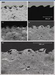
Figure 11: High pixel density, low magnification images of a complex hardfacing alloy on a stainless steel part; enlarged Ni to show fine detail captured in XSI.
Detecting Low Level Compositional Contrast
By reducing the number of pixels in the map but increasing the dwell time per pixel, the number of counts in the pixel spectra can be increased so that the intensity gray scale can be extended. Collecting 2-byte deep data enables imaging of lower concentrations against the background as well as weaker concentration contrast; that is, detection of smaller differences in concentration between closely associated features at any level of concentration. An example of this type of XSI strategy is illustrated in Figure 12 for the Raney nickel alloy previously imaged in Figure 9. In this case, extending the dwell time per pixel enables the Fe constituent, which is present locally at a maximum concentration of 0.04 (mass fraction), to be visualized in the processed image with sensitivity to fine scale spatial details. Moreover, false contrast can be seen in the raw intensity image that arises from the atomic number dependence of the X-ray continuum, producing apparent Fe contrast between the Al-rich and Ni-rich phases, where there is no iron actually present. This false contrast can be nearly eliminated, except for the difference in variance, by performing a background correction by interpolating between background regions set on either side of the FeKα peak.
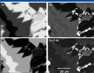
Figure 12: Raney nickel XSI prepared with long pixel dwell (10 ms) to increase X-ray counts per pixel spectrum (~10,000 counts per pixel spectrum).
Visualizing Submicrometer (Nanometer) Scale Compositional Details
Perhaps one of the most striking improvements in X-ray mapping with tFEG-SEM and SDD-EDS is the capability of operating at high spatial resolution. Traditionally, access to high spatial resolution was blocked by the large beam diameter that resulted when large beam currents were required for mapping. Moreover, the delocalization of the X-ray production from the beam impact footprint due to elastic and inelastic scattering that leads to the development of the interaction volume was also considered to negate the possibility of achieving high spatial resolution in bulk (that is, effectively infinitely thick) specimens. In fact, by having the finely focused but high current beam of the tFEG-SEM, the production of X-rays within the footprint of the beam is increased relative to the rest of the interaction volume so as to produce a high spatial frequency that allows the observer to visualize fine details. An example of this is shown in Figure 13, where precipitates in a complex aluminum alloy can be seen with submicrometer resolution.
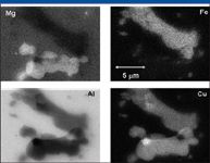
Figure 13: XSI imaging of compositional contrast in complex precipitates in Al alloy 2024-T6.
Conclusions
The analyst equipped with a tFEG-SEM system, an SDD-EDS system ideally optimized for geometric efficiency, and a data mining tool like NIST Lispix can attack the problem of characterizing elemental compositional heterogeneity in a broad range of fields. The previous examples have been drawn from a small sample of those fields, but any condensed matter that can withstand the vacuum requirements of SEM as well as the electron radiation dose (and dose rate) needed to create the XSI database is amenable to study. The examples were also chosen to illustrate some of the different XSI mapping strategies that can be applied to different problems. Indeed, the evolution of the tFEG-SEM/SDD-EDS tool represents such a remarkable step forward that analysts must be prepared to think outside of traditional elemental mapping constraints to fully utilize this wonderful new capability.
Disclaimer
Certain commercial equipment, instruments, or materials are identified in this paper to foster understanding. Such identification does not imply recommendation or endorsement by the National Institute of Standards and Technology, nor does it imply that the materials or equipment identified are necessarily the best available for the purpose.
Dale E. Newbury is with the National Institute of Standards and Technology, Gaithersburg, Maryland.
References
(1) J. Goldstein, D. Newbury, D. Joy, C. Lyman, P. Echlin, E. Lifshin, L. Sawyer, and J. Michael, Scanning Electron Microscopy and X-ray Microanalysis, 3rd ed. (Kluwer Academic Plenum Press, New York, 2003), pp. 1–20.
(2) R. Fitzgerald, K. Kiel, and K. Heinrich, Science 159, 528 (1968).
(3) L. Struder, C. Fiorini, E. Gatti, R. Hartmann, P. Holl, N. Krause, P. Lechner, A. Longoni, G. Lutz, J. Kemmer, N. Meidinger, M. Popp, H. Soltau, and C. von Zanthier, Mikrochim. Acta [suppl.] 15, 11–19 (1998).
(4) D. Newbury, Scanning 27, 227–239 (2005).
(5) D. Newbury, J. Davis, D. Bright, N. Ritchie, J. Michael, and P. Kotula, Microsc. Microanal. 14 (Suppl 2), 1164–1165CD (2008).
(6) S. Davilla, Microsc. Microanal. 13 (Suppl 2), 1344–1345CD (2007).
(7) K.E. Gorlen, L.K. Barden, J.S. Del Priore, C.E. Fiori, C.C. Gibson, and R.D. Leapman, Rev. Sci. Instrum. 55, 912–921 (1984).
(8) D. Bright, NIST Lispix, a software engine for image processing, available free at: http://www.nist.gov/lispix/doc/contents.htm
(9) D.S. Bright and D.E. Newbury, J. Microsc. 216, 186–193 (2004).
(10) P. Kotula, M.R. Keenan, R. Joseph, and J.R. Michael, Microsc. Microanal. 9, 1–17 (2003).

AI Shakes Up Spectroscopy as New Tools Reveal the Secret Life of Molecules
April 14th 2025A leading-edge review led by researchers at Oak Ridge National Laboratory and MIT explores how artificial intelligence is revolutionizing the study of molecular vibrations and phonon dynamics. From infrared and Raman spectroscopy to neutron and X-ray scattering, AI is transforming how scientists interpret vibrational spectra and predict material behaviors.
Advancing Corrosion Resistance in Additively Manufactured Titanium Alloys Through Heat Treatment
April 7th 2025Researchers have demonstrated that heat treatment significantly enhances the corrosion resistance of additively manufactured TC4 titanium alloy by transforming its microstructure, offering valuable insights for aerospace applications.