From Tablets to Teeth: Complete Raman Imaging
Special Issues
Raman imaging has moved on. It is now possible to capitalize on the wealth of information available from a Raman spectrum by imaging materials over large areas, with the spatial resolution, spectral resolution, and laser excitation parameters tailored to suit each application. Raman experiments and images from a diverse range of samples are presented.
Over the last 20 years, the superior chemical specificity and spatial resolution afforded by microRaman spectroscopy has been utilized increasingly in a large number of applications. However, it has failed to meet its full potential for a wide range of sample analyses because of the relatively slow speed of spatial mapping and imaging technologies. New developments in technology have enabled the potential of Raman spectroscopy to elucidate chemical, structural, and distribution information.
With a new system available today (StreamLine fast Raman imaging system, Renishaw plc, Wotton-under-Edge, UK), Raman chemical information can be collected at speeds traditionally associated with IR imaging and laser scanning confocal technologies. The following examples have been selected to inspire spectroscopists to reconsider the types of samples that they can study with Raman spectroscopy.
Complete Pharmaceutical Tablet Imaged in 4 min
Polymorphic identification is one of the critical analytical roles fulfilled by Raman spectroscopy at many stages of the pharmaceutical product design and production process. Confirming that the active ingredient is present within the final product in the correct polymorphic form is crucial, because different polymorphic forms might not exhibit the same clinical benefit to patients. Raman offers unparalleled polymorph discrimination for formulations such as tablets, making Raman imaging particularly suited for the analysis of final stage products. Raman is able to identify the distribution and domain size of an active pharmaceutical ingredient (API), in addition to validating whether any of the processes involved in the preparation of the tablet have affected the polymorphic form adversely.
Figure 1 illustrates the advantages offered by the ability to image at scales ranging from macro to submicrometer. A large-scale image of the complete tablet is used to define further areas of interest to be imaged at higher spatial resolutions. All images were generated using 150 mW of 785-nm laser power, focused into a line to avoid laser-induced sample degradation. In the left-hand image, a 20× objective was selected to image a complete tablet (more than 10,000 spectra), measuring approximately 18 mm × 7 mm, in 4 min. The images on the middle and right show areas of interest at spatial resolutions of approximately 3 μm (20× objective) and 0.5 μm (100× objective), respectively.
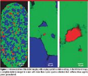
Figure 1
Figure 2 illustrates the Raman images of two tablets of identical size manufactured using the same ingredients. For each image, the tablets were sectioned, and more than 82,000 spectra were collected in 38 min at a spatial resolution of 30 μm. The measurement was performed using 150 mW of 785-nm laser excitation and a dry 20× NA 0.4 (Leica NPlan) microscope objective. The two tablets were taken from batches exhibiting different dissolution profiles. Raman imaging was selected to determine whether the differing dissolution behavior was caused by differences in the tablets' coating layers. However, analysis of the coatings showed that the layers were identical for both tablets. Subsequent imaging of the tablet bulk showed that the variation in the dissolution behavior was caused by differences in the tablet structure, and in particular, the distribution and concentration of one of the components. This case study is a good example of how an enhanced imaging capability can transform the applicability of Raman spectroscopy to solving real-world problems. It was only possible to successfully correlate the dissolution profiles with images generated from the entire tablet. Correlations based upon isolated, smaller regions of the tablet proved to be inaccurate because of the nonuniform domain distribution.
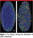
Figure 2
Strain in Semiconductor Devices
Raman is the technique of choice for measuring stress and strain in semiconductor structures. Excess strain can be detrimental to device performance and longevity, but controlled strain is now being engineered into semiconductor devices. The strain induces splitting of the semiconductor's conduction band, resulting in increased electron mobility, which enables the use of higher clock frequencies and gives rise to faster device performance.
A silicon and germanium (SiGe) layer deposited onto a silicon substrate is imaged in Figure 3. The layer is graded such that the germanium fractional content increases from the substrate layer toward the surface. The strain is generated by the substitution of germanium atoms for silicon atoms, giving rise to a mismatch in the crystal lattice. The crosshatch strain pattern revealed by plotting the position of the Si-Si vibration band is not engineered, but is formed at the surface of the Si-Ge layer as a nonhomogenous mechanism of strain relief. The measured maximum shift of 0.2 cm–1 in the Si-Si vibration band corresponds to a strain of approximately 0.1 GPa.
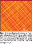
Figure 3
Identification and Characterization of Tooth Decay
Today, most adults and an estimated 90% of school children have experienced tooth decay, with the decline in cases in some developed countries attributed to better oral hygiene practices and preventative measures such as fluoride treatments. Under advice from the British Dental Association, around 6 million people in the UK receive fluorinated water, but there have been some health concerns regarding its use. A safer and more practical strategy would be a targeted approach to prevention, coupled with early-stage diagnosis and treatment. This example illustrates how advanced Raman imaging techniques have a role to play in understanding the mechanisms and chemical changes occurring during the development and treatment of dental caries.
A complete tooth section measuring approximately 9 mm × 16 mm was imaged in under an hour, with greater than 84,000 (216 × 389) spectra collected using a 20× microscope objective. The system described earlier facilitates the use of much higher laser powers than possible with point laser imaging techniques. In this case, it was possible to use 150 mW of 785-nm laser power, a power level that had been shown to destroy the tooth dentine with laser point imaging techniques. The lower laser power required for point-by-point imaging would result in an imaging time in excess of 24 h.
The Raman image in Figure 4 identifies three primary components in the tooth section. Enamel consists almost entirely (> 95%) of mineral, whereas dentine contains 70% mineral and 20% organic material. The primary mineral in all tooth regions is hydroxyapatite, which is crystalline calcium phosphate. As expected, both the enamel and the dentine exhibit the same mineral Raman bands, notably the 960 cm–1 (P-O symmetric stretch) and less intense features between 400 cm–1 and 1100 cm–1. In addition, bands associated with collagen between 800 cm–1 and 3000 cm–1 are measured in the dentine region. These bands are illustrated in Figure 5. The fluorescent regions can be attributed to a higher concentration of bioorganic material.

Figure 4
The horizontal fluorescent feature intersects the edges of the tooth at a position consistent with the position of the cementoenamel junction (CEJ). The CEJ is an anatomical landmark located on the outside of the tooth, at the junction between the enamel, which covers the crown of the tooth, and the cementum, which covers the root of the tooth. This result does suggest a previously unclassified internal transition zone or boundary and is subject to further investigation.
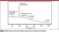
Figure 5
In addition to the enamel and dentine regions, analysis of the data identified a region of fluorescence in the enamel layer. This region, measuring approximately 1.5 mm × 3.4 mm, is imaged at a higher spatial resolution, as illustrated in Figure 6. The data were collected using a dry 20× microscope objective and 150 mW of 785-nm laser power.
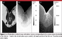
Figure 6
For all images in Figure 6, the following tooth structure applies: the bottom of the image is a small portion of the dentine bulk, the middle "V-shaped" region is the enamel, and the uppermost part of the enamel layer represents the enamel–air interface. Figure 6a is a composite image, in which two images derived from data collected first with parallel, then with crossed polarization sampling geometries, have been combined. It is known that the 960-cm–1 band in sound enamel exhibits a strong polarization dependence, whereas the enamel in a caries region exhibits a less marked polarization dependence. The regions where the peak intensity of the 960-cm–1 band shows a large variation between the two experiments are lightly colored (sound enamel), while regions where the peak area of the 960-cm–1 band shows little variation between the two sampling geometries are colored black (carious region). Curve-fit analysis of the same data reveals frequency and width variation of the 960-cm–1 band between the enamel, dentine, and carious regions. Figure 6b shows the bandwidth of the 960 cm–1 band, with the most striking features being the 4–8 cm–1 bandwidth difference between the enamel and dentine regions and the band sharpening moving toward the outer edge of the enamel region. Figure 6c shows the 960-cm–1 band position, with the carious region exhibiting a shift to a higher wave number, similar to that measured on the outer enamel surface. This suggests that both the outer and carious enamel regions are subject to a similar environment, including episodic acid assault, with periods of destructive demineralization interspersed with natural repair (remineralization) periods.
Raman and Photoluminescence Measurements of Diamond Film
The potential shown by diamond as a material for electronic and optical devices has not been realized fully. The inability to manufacture diamond films that satisfy all of the required electronic and optical properties has meant that it has not been possible to capitalize on some of the unique properties offered by diamond. It is vital that scientists are able to understand the mechanisms of diamond growth and the effect of different growth conditions on the resulting diamond film to overcome this barrier. In the example illustrated in Figure 7, the chemical vapor deposition (CVD) growth method was used to grow a polycrystalline diamond film onto a silicon substrate. The resulting rough growth surface of the film has been polished optically flat, down to within 10 μm of the substrate–diamond growth interface.
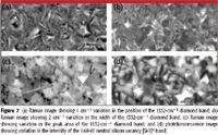
Figure 7
Two sequentially run imaging experiments were analyzed to build the images illustrated in Figure 7. In Figures 7a– 7c, properties of the 1332-cm–1 diamond Raman band are shown, while the intensity of 1.68-eV photoluminescence (PL) band is displayed in Figure 7d. Both these features can be seen in the spectrum shown in Figure 8. The data were collected at room temperature using a 100× objective at 0.5-μm spatial resolution, with 50,000 spectra collected in 15 min. The Raman measurement was performed using 100 mW of 532-nm laser excitation, while a lower power of 10 mW was used for the PL measurement to avoid saturating the detector.
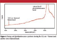
Figure 8
The images represent a wealth of information about the diamond crystals contained within the film, including crystal orientation, crystal shape and quality, defect density, and stress values both within crystal facets and at their boundaries. The letters A and B in Figure 7a are positioned above two interesting features, showing a high density of twinned crystal facets in a fivefold symmetry. It is possible to identify aspects of these features in all figures, with the fivefold symmetry being most evident in Figure 7d. The difference in position of the 1332-cm–1 band at the center of both features suggests that this area is under compressive stress in the feature labeled B, and under tensile stress in the feature labeled A, with an increase in bandwidth suggesting a biaxial nature to the stress. The images generated from the Raman and PL data are good examples of the value added to a flexible microRaman system by the ability to perform rapid imaging experiments. Information such as variation of the band position and the implied crystal stress is only valuable if accompanied by the spatial context offered by the imaging capability. Given the polycrystalline nature of the material, spectra measured at discrete points could yield misleading conclusions about the nature of the film.
Fighting Fraud With the Analysis of Questioned Documents
Raman has proved itself to be a valuable tool in the field of forensic science, primarily as a tool for the nondestructive identification of unknown or suspect substances. A challenging forensic application is one in which two parties disagree on the authenticity of some aspect of a document. Disagreement can center on the order of multiple ink lines, such as signatures. This information can be used to establish whether fraud has taken place, and it might clarify the sequence of any alterations. Techniques such as scanning electron microscopy (SEM), atomic force microscopy (AFM), and a wide range of optical methods have been utilized in attempts to determine which ink was deposited first. However, none of these techniques have been able to reliably validate the order of deposition. In recent blind tests, StreamLine Raman imaging proved to be the most reliable method, giving the correct order of deposition with a better success rate than all other techniques (1).
In the example illustrated in Figure 9, the order of deposition was established for a particularly challenging sample consisting of three crossed ink lines. At the micrometer scale, the paper fibers form a three-dimensional matrix, with the ink distributed at nonuniform thickness at different depths within the matrix. The Raman image is able to distinguish the order, something that is not possible to achieve by studying the white light image.
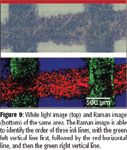
Figure 9
Conclusion
As the preceding examples illustrate, the Raman system described here is a flexible tool, taking full advantage of the analytical possibilities offered by a sophisticated microRaman system. The unique capabilities of the system have expanded the analytical role played by Raman spectroscopy in existing application areas such as the analysis of pharmaceutical and semiconductor materials. In addition, it has inspired new methodologies in both forensic science (1) and hospital laboratories undertaking feasibility studies to improve histological diagnosis (2).
Acknowledgments
We would like to thank Dr. Christian Zakian from the Dental Health Unit, The University of Manchester, for his contribution to the Raman imaging study of detailed structural and chemical information relating to a whole tooth. We would like to thank Mike Ansell, an experienced forensic document examiner, for his contribution to the document analysis project.
Geraint Evans, Tim Smith, and Matthew Bloomfield are with Renishaw plc, Wotton-under-Edge, UK.
References
(1) Results to be presented by Tim Smith and Mike Ansell at the forensic science service (FSS) conference, 4th–6th July 2008, Nottingham, UK.
(2) Biophotonics Research Group, Gloucestershire Hospitals NHS Foundation Trust, Gloucester, UK.

AI-Powered SERS Spectroscopy Breakthrough Boosts Safety of Medicinal Food Products
April 16th 2025A new deep learning-enhanced spectroscopic platform—SERSome—developed by researchers in China and Finland, identifies medicinal and edible homologs (MEHs) with 98% accuracy. This innovation could revolutionize safety and quality control in the growing MEH market.
New Raman Spectroscopy Method Enhances Real-Time Monitoring Across Fermentation Processes
April 15th 2025Researchers at Delft University of Technology have developed a novel method using single compound spectra to enhance the transferability and accuracy of Raman spectroscopy models for real-time fermentation monitoring.
Nanometer-Scale Studies Using Tip Enhanced Raman Spectroscopy
February 8th 2013Volker Deckert, the winner of the 2013 Charles Mann Award, is advancing the use of tip enhanced Raman spectroscopy (TERS) to push the lateral resolution of vibrational spectroscopy well below the Abbe limit, to achieve single-molecule sensitivity. Because the tip can be moved with sub-nanometer precision, structural information with unmatched spatial resolution can be achieved without the need of specific labels.