A Comprehensive Study of WSe2 Crystals Using Correlated Raman, Photoluminescence (PL), Second Harmonic Generation (SHG), and Atomic Force Microscopy (AFM) Imaging
Tungsten diselenide (WSe2) is a transition metal dichalcogenide (TMDC) that belongs to a class of nanomaterials with potential in optoelectronic device applications. Several characteristics that define the electronic, optical, and thermal properties of these two-dimensional (2D) crystals are thickness, crystal symmetry changes, and growth defects. The combination of various techniques for investigating the same WSe2 flake sample shows that various processes involved in producing the photoluminescence (PL) signal are correlated with the localized strain. The WSe2 flake samples are observable by confocal Raman imaging and topographic homogeneity can be determined by atomic force microscopy (AFM). The edge of the flake shows strong variations, which could be explained by the correlation of the various techniques. In addition, second harmonic generation (SHG) measurements identify grain boundaries as potential sources of strain relief, which is in agreement with both the confocal Raman as well as the confocal PL results.
Transition metal dichalcogenides (TMDCs) are a family of materials with an MX2 composition, consisting of metallic (M = W, Mo, Nb, and Ta) and chalcogen (X = S, Se, and Te) atoms. They are arranged in layered structures in the form X-M-X and are considered as a single monolayer, with the chalcogen atoms in two hexagonal planes separated by one plane of transition metal atoms (1–5). Similar to graphene, they can be exfoliated to one or few layered materials or grown using different growth methods such as chemical vapor deposition (CVD). These single- or few-layer materials exhibit unique electronic and optical properties, which are significantly different from the bulk precursor. Bandgaps of semiconducting TMDCs can be tuned by changing the number of layers, the chemical composition, or the strain of the materials (1–8). Their possible applications include the production of transistors, photodetectors, light emitting diodes (LEDs), and photovoltaic cells (9,10).
To produce high-quality devices, the synthesis processes must be evaluated efficiently. Nondestructive imaging techniques are required for monitoring crystal properties and features such as grain boundaries, layer numbers, defect densities, and doping and strain fields. In many cases, a combination of measurement techniques, such as the ones outlined below, leads to a more thorough understanding of the properties of these materials.
Atomic force microscopy (AFM) is widely used to characterize the topographic composition of 2D materials. It determines the number of monoatomic steps and ripples in the z-direction, and resolves lattice orientations and surface defects in the xy-plane. It can also reveal nanomechanical, nanoelectromechanical, or nanoelectrochemical properties of 2D materials (11–15).
Raman and photoluminescence (PL) spectroscopy and imaging are nondestructive techniques that reveal the lattice dynamics of single-layer and multilayer TMDCs and enable the determination of their electronic structures (1,5,15–22).
Second harmonic generation (SHG) imaging is a technique sensitive to changes in crystal orientation and symmetry. It can visualize grain boundaries, and polarization-dependent SHG measurements are often used to reveal strain fields by rotating the polarization direction of the excitation light while recording the intensity of the correspondingly polarized SHG signal component (1,4,6–8,23–26).
In this study, the combination of the abovementioned techniques made possible the correlation of strong, localized changes in PL signals on the outer edge of the observed WSe2 crystals with strain in the lattice as well as topographic inhomogeneities. It was also possible to correlate the absence of strain and the absence of the changes in PL in locations where it could have been expected, with the location of grain boundaries as observable through SHG.
Materials and Methods
Samples of WSe2 were grown at atmospheric pressure and 900 °C directly on SiO2/Si substrates by solid-source CVD using selenium and WO3 precursors, as previously reported (27). The WSe2 crystals were predominantly monolayered with small overgrown bilayer regions commonly found with this growth method. All experiments were performed using an alpha300 RA confocal Raman AFM microscope at room temperature (WITec). AFM measurements were performed in AC mode with a force modulation cantilever (Nanosensors) with a nominal spring constant of 2.8 N/m and a nominal resonance frequency of 80 kHz.
For confocal Raman and confocal PL measurements, the alpha300 microscope was equipped with a 100x (NA = 0.9) Epiplan Neofluar Zeiss objective, a 532-nm excitation laser with a power before the objective of 2 mW, and a UHTS300 VIS spectrometer (28). The spectrometer was equipped with various gratings mounted on a motorized turret. The 1800 g/mm grating allowed for a resolution of better than 1 cm-1 and was used for high resolution Raman imaging, whereas a 300 g/mm grating with a resolution better than 3 cm-1 (0.33 meV) was used for PL measurements.
For confocal SHG measurements a fiber-coupled linear-polarized 7.8 ps pulsed laser (λ = 1064 nm) was used as the excitation source. The same objective for the Raman measurements was used to focus the pulsed laser with a spot size of approximately 700 nm onto the sample. The reflected optical signal was collected with the same objective, transmitted via photonic fiber and then directed into the UHTS300 VIS spectrometer. A 950 nm short-pass filter was used before the pinhole to block the excitation laser beam. The SHG signal for this setup is detected at 532 nm, corresponding to half of the fundamental excitation wavelength of 1064 nm.
Polarization-dependent SHG measurements were performed by adding a super-achromatic λ/2 retarder plate on a motorized rotation mount in the beam path before the objective as well as a retractable linear polarization filter in the detection beam path in front of the pinhole.
Results and Discussion
AFM Imaging
Figure 1 shows the (a) AFM topography map, (b) line scans, and (c) phase image of the studied WSe2 crystal. The marked cross sections (cs1 and cs2) are shown in Figure 1b. The topography image reveals a 0.7 ± 0.1 nm step height of the WSe2 crystal, corresponding to a monolayer deposited on the Si/SiO2 substrate, in good agreement with previously reported studies (12,13,15). The topographically elevated triangular structures are about 2 nm higher than the monolayer, corresponding to a fourfold-layered crystal. Besides the large fourfold-layered crystal in the center, smaller crystals of the same height are also visible and are marked with arrows in Figure 1a. The side length of such a small triangle is in the range of 350–400 nm. The simultaneously recorded phase image reveals a down-shift for the monolayer whereas the fourfold-layered region shows the same contrast as the substrate. The smaller triangles also show a similar phase shift indicating that the same material is likely to be present there. Such phase shifts in AC mode for AFM images are associated with a change in the viscoelastic properties of the material, indicating that the fourfold layers are similar in those properties to the substrate, whereas clear differences are visible for the single layer.
FIGURE 1: (a) Atomic force microscopy (AFM) topography image, including (b) cross sections marked in the topography image, and (c) phase image of the studied WSe2 crystal CVD-grown on a Si/SiO2 substrate. The arrows in the topography image indicate the positions of small triangular structures.
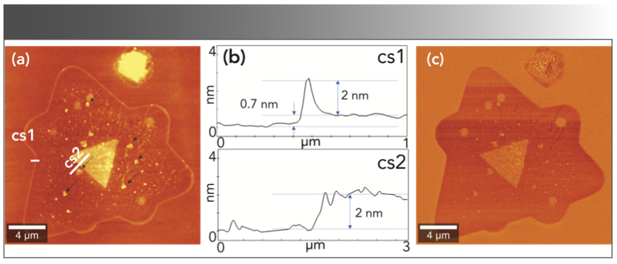
The rounded edges of the monolayer crystal are also of interest, which developed because of the temperature and precursor fluxes during growth conditions (12). These two factors have been shown to have a significant impact on monolayer morphology in MoS2, a TMDC with similar structure to WSe2 (29). The monolayer crystal is surrounded by a 2 nm high edge. The width of the edge is in the range of 150 nm. It is only in the convex-rounded corners that a substantially increased width to approximately 300 nm is detected. The phase image is for the entire edge similar to the monolayer value, which indicates that the viscoelastic properties of the edge are similar to those of the monolayer. Thus, the 2 nm height of the edge is unlikely to be a result of multilayer growth in this area.
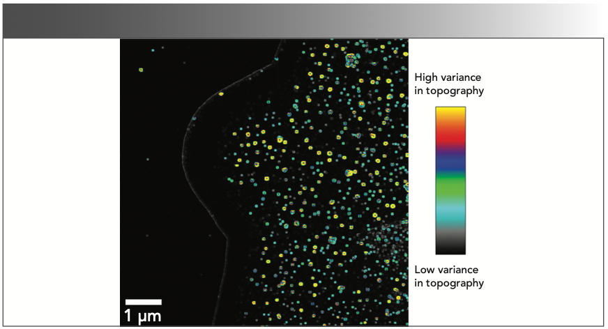
In Figure 1a, it can be seen that the area directly inside the elevated edge is the flattest area on the flake. To illustrate this further, a zoom-in scan was performed and the variance of the topography signal was evaluated (Figure 2). It can clearly be seen that just inside the flake, an area of about 1 μm in width shows a much smaller variance in topography than the rest of the flake. Because only the inner part of the flake shows higher topographical variance, sample contamination can be excluded as the cause.
FIGURE 2: AFM topography variance of a zoomed-in area of the flake. The uniform area on the inside of the elevated edge (faint gray line) can be seen clearly.
Confocal Raman Imaging
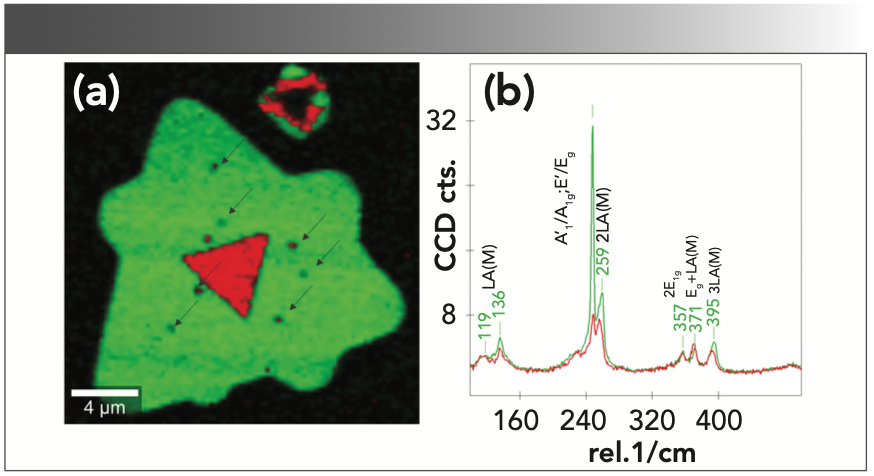
Raman spectroscopy of WSe2 crystals obtained by exfoliation or various growth methods is widely represented in literature (5,16–21,30), whereas few references can be found for confocal Raman imaging of WSe2 (12,14,22). The same crystal as shown in Figure 1 was measured in confocal Raman imaging mode using the parameters listed in Figure 3. The presented Raman spectra were evaluated from a 2D array of Raman spectra using multivariate spectral analysis methods (31). As expected, the Raman spectra (Figure 3b) associated with the monolayer (green) and fourfold layer (red) show different characteristics, as described previously using Raman spectroscopy and theoretical calculations (20,21,30). The Raman image (Figure 3a) reveals the presence of the monolayer displayed in green and the fourfold-layered crystals in red. Although the small crystals (marked with arrows) have a baseline of only 350–400 nm as shown in the AFM image, they provide enough signal to be detected in the Raman image with a confocal Raman microscope. The edge shows the same Raman spectrum as the inner monolayer. Therefore, it confirms the assumption made based on the AFM results, that the small triangles are fourfold crystals, whereas the edge with its elevated height cannot be explained by a multilayer effect.
FIGURE 3: (a) Color-coded Raman image and the (b) corresponding Raman spectra evaluated from the two-dimensional (2D) array of spectra. Raman imaging parameters: 30 x 30 μm2, 120 x 120 pixels, Raman excitation laser 532 nm, laser power 2 mW, integration time per spectrum 0.1 s, 1800 g/mm grating.
Furthermore, by fitting Lorentzian curves to the Raman band at about 248 cm-1 for all 14,400 acquired Raman spectra, the precise peak position for every location on the flake was obtained (Figure 4a). It reveals a relatively uniform peak position over the monolayer at ~247.8 cm-1, whereas at the edges a small red shift of ~0.34 cm-1 can be determined. Figure 4b shows the histograms evaluated from the monolayer without the edge and four- fold layer (blue), and also from the edge only (green). This clearly shows the shift in peak position of the E’/Eg Raman band, characteristic for in-plane molecular vibrations in WSe2, and associated in literature with strain of the monolayer (32). The fourfold-layer crystal is associated with a larger red shift compared to the monolayer, in good agreement with the literature (20). The width of the Raman band (Figure 4c) does not show specific, detectable changes between the monolayer and the edge, confirming the presence of one crystal with strained edges (15).
FIGURE 4: Raman analysis. (a) Map of fitted Raman band around 248 cm-1 showing peak shifts at the rounded edges of the crystal. (b) Histograms of the Raman band positions acquired from the monolayer without the edges and from only the edges. (c) The width of the analyzed Raman band does not show significant changes between the monolayer and the edges.

Confocal PL Imaging
Figure 5 shows the color-coded PL image of the studied WSe2 crystal, measured with the parameters listed in the figure caption. The presented PL spectra were evaluated from the 2D array of spectra using multivariate spectral analysis methods (31). The colors in the image of Figure 5 match the colors of the spectra next to it. The monolayer shows a uniform PL distribution (shown in blue). The PL intensity of the fourfold crystal is shown in green and is, as expected, much weaker. According to bandgap calculations reported in the literature (16), the monolayer of WSe2 is a direct bandgap semiconductor. Multilayer WSe2 crystals however are indirect band gap semiconductors that display decreased photoluminescence intensity compared to monolayers. This could be detected in the central triangle, as well as for the small triangles indicated again with arrows in Figure 5. At the entire edge of the crystal, an increase of the PL intensity could be observed. The highest PL intensity was found at the convex edge, where Raman imaging revealed the highest strain in the monolayer (see Figure 4).
FIGURE 5: (a) Color-coded confocal photoluminescence (PL) image and the (b) corresponding PL spectra evaluated from the 2D array of spectra. PL imaging parameters: 30 x 30 μm2, 120 x 120 pixels, excitation laser 532 nm, laser power 2 mW, integration time per spectrum 0.05 s, 300 g/mm grating.
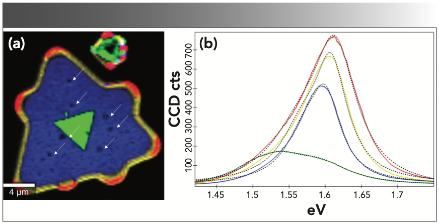
All measured PL spectra have an asymmetric curve form, indicating that more than one process is contributing to the PL emission (15). With defect density distribution having an impact on the level of degeneration observed in the involved layers, varying numbers of fit curves were used (15,16). For the present case, fitting three Lorentzian curves to the PL spectra provided a good description of the experimental data. The fits are presented as dashed lines in Figure 5 and follow the experimentally obtained data (colored curves) well. The characteristic features, such as peak position, width, and area, of these Lorentzian fits are presented in Figure 6. According to Fang and others (15), the three Lorentzian functions fitted to the PL spectra correspond to three different emission processes: The neutral exciton at about 1.62 eV, a trion at 1.6 eV, and a defect emission caused by lattice defects at about 1.53 eV. Figure 6 shows (a) the positions, (b) area and (c) width of the three individual peaks into which each measured curve is deconvoluted. The errors based on the fitting algorithm are indicated and where they are smaller than the displayed markers in the figure.
FIGURE 6: PL spectra evaluation: (a) the peak positions, (b) the area, and (c) the full width at half maximum of individual Lorentzian fits used to deconvolute each measured curve (triangles = neutral exciton peak; squares = trion peak and diamonds = defect peak).
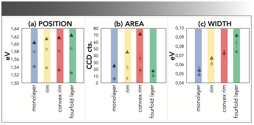
For the monolayer, we can observe a consistent shift to lower energies of approximately 25 meV for the neutral exciton and the trion peak compared to the literature (15), whereas the defect peak appears at approximately 10 meV higher energy.
For the edge, no significant changes in the position of the trion peak were observed, whereas the position of the neutral exciton is upshifted relative to the monolayer. The defect band is downshifted for the edge and even further downshifted for the convex edge. The area plot (Figure 6b) shows a clear increase in the intensities for the convex edge for all three peaks, whereas for the remaining edge, only the peak associated with the neutral exciton seems substantially increased. The width of the peaks (Figure 6c) seems to increase similarly for all three peaks with the monolayer being the narrowest and the convex edge being the broadest.
The enhancement of the defect peak intensity for only the convex edge fits well with the increased strain as observed from the Raman measurements because a higher strain may be associated with a higher defect density. The change in the width of the fitted peaks may reflect the level of uniformity in the respective areas.
Confocal SHG Imaging
Figure 7 shows the results of confocal SHG microscopy measurements of the analyzed WSe2 crystal. The monolayer reveals a strong SHG signal, whereas the fourfold layer shows a small signal (integrated intensity of the SHG peak near 532 nm) as highlighted in the image (Figure 7a). As with most TMDCs, WSe2 belongs to the point group D6h, in the 3R phase with two Se-W-Se unit cells of trigonal prismatic coordination (5). For odd layers (such as the monolayer) the lack of inversion symmetry gives rise to finite second-order nonlinearity. An even numbers of layers (such as the fourfold layers) show little or no second-order nonlinearity (4,23).
FIGURE 7: SHG analysis of the studied crystal. (a) Integrated intensity image of the SHG signal; (b) SHG signal from the Si-substrate (pink), monolayer (blue) and fourfold layer (green). (c) Polar plots of the SHG signal intensity as a function of the excitation polarization angle at the color-coded marked positions. SHG imaging parameters: 30 x 30 μm2, 120 x 120 pixels, pulsed 1064 nm laser, laser power: 28 mW, 0.1 s integration time per pixel.
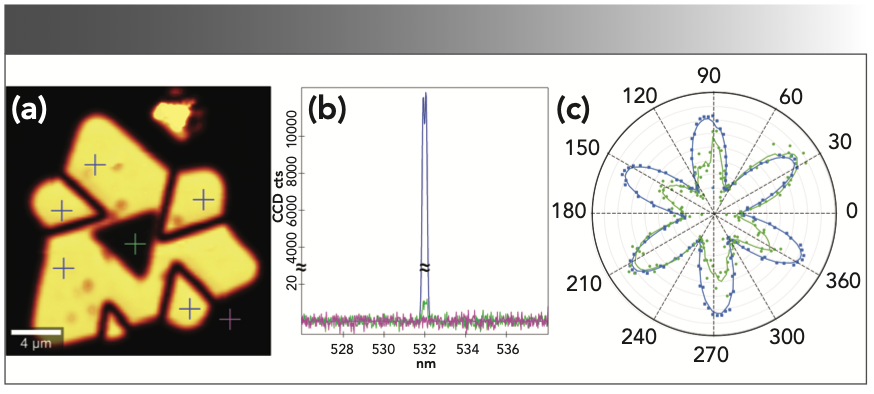
The SHG intensities acquired from the monolayer (blue), the fourfold-layered crystal (green) and silicon-substrate (purple) are shown in Figure 7b. These data reveal an enhancement of the nonlinear SHG signal of the WSe2 monolayer by three orders of magnitude compared to the fourfold-layered crystal, which is in good agreement with previously reported second-order susceptibility measurements on exfoliated WSe2 (1). Although the analyzed crystal shows uniform Raman (Figure 3) and PL (Figure 5) signals over the entire monolayer, the SHG image reveals the polycrystalline nature of the monolayer because the SHG signal is substantially lower at the grain boundaries. The incident polarization of the pump laser is approximately along the x-axis of the SHG-image (Figure 7a) and the total second harmonic radiation is collected. For these measurements the linear polarization filter in the detection beam path was removed. The uniform SHG intensity within each grain indicates that the individual grains are single crystals. At the grain boundaries, the SHG is suppressed as a result of the destructive interference and annihilation of the waves generated from the neighboring grains with different orientations (24,25). Although the grain boundaries are only a few atoms in width, the crystal boundaries can be clearly visualized. Similar results are reported from monolayers of molybdenum disulfide (MoS2) as a result of different chirality of the stitching areas of the domains of neighboring crystals (24,25).
Polarization measurements were carried out at the individual grains and their positions are marked with blue crosses (Figure 7a). They all show the same six- fold symmetry with the same orientation, depicted as the blue curve in the polar plot (Figure 7c). The polarization series shown in green (Figure 7c) was acquired from the fourfold-layered crystal. The intensity of this second-harmonic signal is three orders of magnitude smaller than that of the monolayer. It was plotted at a magnified intensity to reveal the differences in the relative intensities of the lobes.
Summary
The WSe2 crystal was analyzed with AFM, confocal Raman, PL, and SHG microscopy. The overlay of the images acquired by the different techniques is presented in Figure 8 and visualizes the complementary findings from the techniques used. Figure 8a shows the overlay of the AFM and PL images. From this view, it can be seen that the area with high topographic variance (compared with Figure 2) correlates extremely well with the area of the enhanced PL in the edge area. Figure 8b shows the overlay of the SHG and PL images. This view indicates that the concave corners of the flake correlate with grain boundaries and that at these positions, no change of the PL signal relative to the remaining edge can be seen. From this, it may be concluded that the stress level at the grain boundaries is significantly lower than at the rounded edges. This finding is in agreement with the Raman findings as well (Figure 4). Although the slightly elevated topography at the edges may play a role in the edges’ PL signal, it seems more likely that the flat topography as well as the stress on the convex corners plays the more significant role. In Figure 8c, the SHG image is overlaid onto the AFM topography, showing the polycrystalline nature of the analyzed WSe2 monolayer. The AFM image does not reveal detectable topographic changes at the grain boundaries and the SHG–AFM combination additionally shows that the SHG intensity decreases in a similar manner at the outer edges as it does at the internal grain boundaries.
FIGURE 8: Overlay of images obtained with various techniques: (a) AFM and PL, (b) SHG and PL and (c) AFM and SHG.
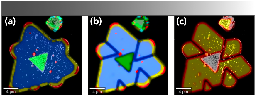
By combining the various techniques, it was possible to obtain a better understanding of the sample than would have been possible by only employing the individual techniques in isolation. It was especially interesting that a topographically flat edge of about 1 μm in width shows an enhanced PL signal, where only the neutral exciton emission seems to be enhanced. The rounded edges show additional PL enhancement of all postulated processes and exhibit a clear shift of the Raman peaks, indicative of increased stress in these areas. By adding SHG as a fourth measurement technique, the multicrystalline nature of the flake became apparent and the concave edges could be identified as grain boundaries, which explains why the PL signal was not increased here and the Raman did not show an enhanced strain.
References
(1) J. Ribeiro-Soares, C. Janish, Z. Liu, A.L. Elias, M. S. Dresselhaus, M. Terrones, L. G. Cancado, and A. Jorio, 2D Mater. 2, 45015 (2015).
(2) R. Zhang, H. Li, G. Hao, W. Liu, Y. Ye, Z. Li, X. Yuan, and C. Liu, Key Eng. Mater. 765, 16–23 (2018).
(3) M. Ye, D. Winslow, D. Zhang, R. Pandey, and Y.K. Yap, Photonics 2, 288–307 (2015).
(4) Y. Wang, J. Xiao, S. Yang, Y. Wang and X. Zhang, Opt. Mater. Express 9, 1136 (2019).
(5) R. Saito, Y. Tatsumi, S. Huang, X. Ling, and M. S. Dresselhaus. J. Phys. Condensed Matter 28, 353002 (2016).
(6) C. Janish, Y. Wang, D. Ma, N. Mehta, A.L. Elias, N. Perea-Lopez, M. Terrones, V. Crespi and Z. Liu, Sci. Rep. 4, 5530 (2014).
(7) X. Li, W. Liu, Y. Song, C. Zhang, H. Long, K. Wang, B. Wang, and P. Lu, Adv. Optical Mat. 10, 1801270 (2018).
(8) H. Chen, V. Corboliou, A. S. Solntsev, D.Y. Choi, M. A. Vincenti, D. de Ceglia, C. de Angelis, Y. Lu, D. N. Neshev, Light Sci. Appl. 6, 17016 (2017).
(9) W. Choi, N. Choudhary, G. H. Han, J. Park, D. Akinwade, and Y. H. Lee, Materials Today 20, 116 (2017).
(10) H. Chen, Y. Tang, T. Jiang, and G. Li, Comprehensive Nanosci. Nanotech. 1 (2019).
(11) H. Zhang, J. Huang, Y. Wang, R. Liu, X. Huai, J. Jiang, and C. Anfuso, Opt. Commun. 10, 1016 (2017).
(12) B. Liu, M. Fathi, Liang Chen, A. Abbas, Y. Ma and C. Zhou, ACS Nano 9, 6119–6127 (2015).
(13) S. Tongay, J. Suh, C. Ataca, W. Fan, A. Luce, J.S. Kang, J. Liu, C. Ko, R. Raghunathanan, J. Zhou, F. Ogletree, J. Li, J. C. Grossmann, and J. Wu, Sci. Rep. 3, 2657 (2013).
(14) H.S. Jang, J.Y. Lim, S.G. Kang, S.H. Hyun, S. Sanhu, S.K. Son, J.H. Lee, and D. Whang, Nanomaterials 9, 1642 (2019).
(15) L. Fang, H. Chen, X. Yuan, H. Huang, G. Chen, L. Li, J. Ding, J. He, and S. Tao, Nanoscale Res. Lett. 14, 274 (2019).
(16) H. Sahin, S. Tongay, S. Horzum, W. Fan, J. Zhou, J. Li, J. Wu, and F.M. Peeters, Phys. Rev. B 87, 165409 (2013).
(17) W. Shi, M.L. Lin, Q.H. Tan, X.F. Qiao, J. Zhang, and P.H. Tan, 2D Mater. 3, 25016 (2016).
(18) P. Tonndorf, R. Schmidt, P. Böttger, X. Zhang, J. Börner, A. Liebeig, M. Albrecht, C. Kloc, O. Gordan, D. R. T. Zahn, S.M. de Vascocellos, and R. Bratschitsch, Optics Express 21, 4908 (2013).
(19) W. Zhao, Z. Ghorannevis, A. K. Kumar, J. R. Pang, M. Toh, X. Zhang, C. Kloc, P.H. Tan, and G. Eda, Nanoscale 5, 9677–9683 (2013).
(20) E. Del Corro, H. Terrones, A. Elias, C. Fantini, S. Feng, M.A. Nguyen, T.E. Mallouk, M. Terrones, and M. Pimenta, ACS Nano 8(9), 9629–9635 (2014).
(21) H. Terrones, E. Del Corro, S. Feng, J. M. Poumirol, D. Rhodes, D. Smirnov, N.R. Pradhan, Z. Lin, M.A.T. Nguyen, A. L. Elias, T. E. Mallouk, L. Balicas, M. A. Pimenta, and M. Terrones, Sci. Rep. 4, 4215 (2014).
(22) M. O ́Brian, N. McEvoy, D. Hanlon, T. Hallam, J.N. Coleman, and G. Duesberg, Sci. Rep. 6, 19476 (2016).
(23) L. Malard, T.V. Alencar, A.P.M. Barboza, K.F. Mak, A.M. dePaula, Phys. Rev. B. 87, 201401 (2013).
(24) X. Yin, Z. Ye, D.A. Chennet, Y. Ye, K. O`Brien, J.C. Hone, and X. Zhang, Science 344, 88–490 (2014).
(25) H. Hu, Z. Yang, L. Du, J. Zhang, J. Shi, W. Chen, P. Vhen, M. Liao, J. Zhao, J. Meng, G. Wang, J. Zhu, R. Yang, D. Shi, L. Gu, and G. Zhang, Small 13, 1603005 (2017).
(26) Y. Li, Y. Rao, K.F. Mak, Y. You, S. Wang, C.R. Dean, T.F. Heinz, Nano Letters 13, 3329–3333 (2013).
(27) J. Chen, C.S. Bailey, Y. Hong, L. Wang, Z. Cai, L. Shen, B. Hou, Y. Wang, H. Shi, J. Sambur, W. Ren, E. Pop, S. Cronin, ACS Photonics 6, 787–792 (2019).
(28) T. Dieing and O. Hollricher, Vib. Spectrosc. 48, 22-17 (2008).
(29) S.Y. Yang, G.W. Shim, S. Seo, and S. Choi, Nano Res. 10, 255–262 (2017).
(30) X. Luo, Y. Zhao, J. Zhang, M. Toh, C. Kloc, Q. Xiong, and S. Y. Quek, Phys. Rev. B. 88, 195313 (2013).
(31) T. Dieing and W. Ibach, in Confocal Raman Microscopy, T. Dieng, and O. Hollricher J. Toporski, Eds. (Springer, Heidelberg, Germany, 2019), pp. 89–121.
(32) Y. Wang, C. Cong, C. Qiu, and T. Yu, Small 10, 1002 (2013).
Ute Schmidt, Jan Englert, Olaf Hollricher, and Thomas Dieing are with WITec GmbH in Ulm, Germany. Eilam Yalon and Guy Ankonina are with the Department of Electrical Engineering at Technion in Haifa, Israel. Eric Pop and Connor Bailey are with the Department of Electrical Engineering at Stanford University in Stanford, California. Direct correspondence to: ute.schmidt@witec.de. ●

AI-Powered SERS Spectroscopy Breakthrough Boosts Safety of Medicinal Food Products
April 16th 2025A new deep learning-enhanced spectroscopic platform—SERSome—developed by researchers in China and Finland, identifies medicinal and edible homologs (MEHs) with 98% accuracy. This innovation could revolutionize safety and quality control in the growing MEH market.
New Raman Spectroscopy Method Enhances Real-Time Monitoring Across Fermentation Processes
April 15th 2025Researchers at Delft University of Technology have developed a novel method using single compound spectra to enhance the transferability and accuracy of Raman spectroscopy models for real-time fermentation monitoring.
Nanometer-Scale Studies Using Tip Enhanced Raman Spectroscopy
February 8th 2013Volker Deckert, the winner of the 2013 Charles Mann Award, is advancing the use of tip enhanced Raman spectroscopy (TERS) to push the lateral resolution of vibrational spectroscopy well below the Abbe limit, to achieve single-molecule sensitivity. Because the tip can be moved with sub-nanometer precision, structural information with unmatched spatial resolution can be achieved without the need of specific labels.
2 Commerce Drive
Cranbury, NJ 08512
All rights reserved.