Analysis of Solar Silicon Using High-Throughput Spectroscopy
Special Issues
Infrared spectroscopy is a powerful analysis technique used in the semiconductor industry to ensure the quality of silicon and silicon wafers. The authors discuss the use of an inexpensive, lab-based system to measure carbon and oxygen concentrations in silicon to the level of precision required by the solar silicon industry.
Infrared spectroscopy is a powerful analysis technique used in the semiconductor industry to ensure the quality of silicon and silicon wafers. An extensive set of ASTM test methods has been developed defining methods for silicon used in the electronics industry (now administered by SEMI, a global industry association for silicon device producers). The recent emphasis on non-hydrocarbon-based energy production has increased the interest in solar silicon applications, which in turn brought about a need for a rapid, sensitive, and well-characterized analysis tool. Although the requirements for silicon used in photovoltaic solar cells are slightly different from those used in electronics, many of the material specifications are similar.
One of the most important questions for silicon producers involves the determination of the amount of oxygen and carbon in the silicon. During the crystal growth process, oxygen and carbon are introduced in varying degrees into the molten silicon from the quartz crucible and the graphite heaters. As the ingot is pulled from the melt and the silicon solidifies, these impurities become incorporated into the crystal lattice. Because the carbon atoms occupy sites normally taken by silicon atoms in the lattice structure, this type of impurity is classified as substitutional. In addition, the oxygen atoms can find positions within the lattice structure between the silicon atoms, forming interstitial impurities. Different levels of interstitial oxygen (Oi) in the silicon have been correlated with varying effects, both physical and electrical. The requirement to control these effects leads to the need for monitoring the concentration of Oi in the wafers used to fabricate devices. Although no direct effects of the substitutional carbon (Cs) have been proven, many experiments suggest that Cs affects the way the Oi behaves when silicon is heated, such as in typical silicon-processing temperature cycles. Carbon can lead to defect formation and the formation of swirls as well as assist the precipitation of oxygen.
The increased production of solar silicon has led to a requirement for a technique to quickly analyze the material from the ingot before final processing. To improve productivity, the analysis must analyze the C and O concentrations from multiple samples with minimal user interaction. The desired instrument should allow an operator to determine easily if a specific sample is "out-of-spec." These characteristics, coupled with the existing knowledge of silicon analysis from the electronics industry, make infrared a leading candidate. Here, it is shown how an accessory initially designed for analyzing biotech samples using the standard 96-well-plate format can be used to measure carbon and oxygen concentrations in silicon to the level of precision required by the solar silicon industry. This accessory permits users to analyze samples arranged in a precise X,Y array and can be customized for any array of samples that fit within the constraints of the stage movement and beam size of the spectrometer.
Production tools used in fabrication centers have rigid requirements, which lead to high costs. The needs of the burgeoning solar silicon industry are better met with an inexpensive, laboratory-based tool, used in a quality control laboratory rather than in a fabrication center. This is the focus of the system discussed here.
Experimental
A Fourier-transform infrared (FT-IR) system (Nicolet 6700 FT-IR spectrometer, Thermo Fisher Scientific) was fitted with a plate reader directly into the sample compartment (Microwell plate reader, Thermo Fisher Scientific). The plate reader was configured to analyze 40 samples of silicon that are 10 mm in diameter and 2 mm thick.
The accessory consists of a high-precision X,Y stage controlled via array automation software (OMNIC Array Automation, Thermo Fisher Scientific). The optical module contained an integrated camera for recording a visual record. A special cover with a small door allows the sample plate to be accessed without opening the cover (no need to break purge). The software also permits the integration of the metrology procedure. The results can be color coded using the metrology results. Thresholds can be assigned so that any samples that exceed the upper limit are colored red and any samples below the lower limit are colored purple, providing the instant feedback required for pass–fail determination.
Spectra were acquired from various silicon samples at a resolution of 4 cm–1. The analytical methods used to measure the carbon and oxygen concentrations are based upon the test methods originally developed by the ASTM and now supported by SEMI (MF1188-1107 and MF1391-1107). Figure 1 shows the spectrum of the 2-mm-thick float zone reference wafer and the spectra of the carbon and oxygen references after the silicon peaks have been removed. This spectral subtraction and intensity measurement forms the basis of the ASTM/SEMI methods. The intensity of the oxygen band at 1107 cm–1 is scaled to determine the oxygen concentration, and the band at 607 cm–1 is used to determine the substitutional carbon. The ASTM/SEMI methods require 2-mm-thick samples that have been double side polished. A further software package was used to perform the accurate analysis of samples of difference thicknesses (ECO/RS, Thermo Fisher Scientific).
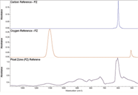
Figure 1: Carbon and oxygen float zone (ultrapure) standards and reference spectrum.
Performance Verification
To verify the performance of the accessory for silicon analysis, spectra were acquired from a set of NIST Standard Reference Material 2551 oxygen in silicon samples. The set consists of four 25-mm-square, 2-mm-thick silicon samples, mirror polished on both sides. A high resistivity float zone material with negligible oxygen content serves as the reference. The remaining three samples are cut from n-type crystals grown by a modified Czochralski process. The room temperature resistivity is >3 ohm-cm and the nominal oxygen concentrations are 17, 23, and 26 parts per million atomic (ppma). The samples were positioned in the Microwell plate reader in a 2 × 2 array and the locations were entered into the software. Figure 2 shows the array automation analysis of the four samples. The wells in the schematic in the upper left are colored based upon the concentration of oxygen in the sample calculated using one of the ECO/RS proven methods. The calculated values used to determine the color of each well are as follows: A1: 0.0 ppma, B1: 17.45 ppma, A2: 23.50 ppma, and B2: 26.90 ppma. The lower portion of the display contains the overlay of the spectra from the four samples showing the differences in the oxygen peak at 1107 cm–1.
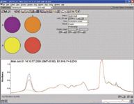
Figure 2: Reference samples run using the array automation software. The color-coded results permit instant visual confirmation of the passâfail status.
The precision and stability of the system were evaluated using the standard with the highest oxygen concentration (26.303 ppma) as reported by NIST. A total of 50 repeat spectra were acquired using 4 cm–1 resolution and 128 scans. The carbon and oxygen concentrations were determined and the results stored automatically. The average value for the 50 measurements was 26.629 ppma oxygen with a standard deviation of 0.083 ppma.
Setting Up and Measuring 10 mm × 2 mm Disks
Seven samples were positioned onto a specially designed, 40-position sample holder with 10-mm slots. The array automation software contains a template tool permitting data collection from any custom plate design. FT-IR data were collected and an analysis based upon a predefined ASTM/SEMI method was performed. Figure 3 shows the results of the analysis. The images for each sample are captured during the data collection. This allows users to peruse all aspects of the collection — spectra, images, and results — in one interface. Note that one sample — shown in orange — had a much higher concentration of carbon (6.3 ppma) than the others.
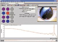
Figure 3: Analysis of silicon samples, showing visual image, spectra, and numerical results.
Measuring Multiple Points on a Larger Sample
The plate reader was designed to measure discrete samples in an array. However, it can also be used to measure multiple points on a single sample or on multiple samples that fit within the 125 mm × 85 mm stage mount. For example, Figure 4 shows the measurement of an 8 × 12 array of points on a silicon test wafer. The results are overlaid on a display of the schematic showing the relative concentrations of oxygen across the sample. The standard deviations for both the carbon and the oxygen are less than 0.1 ppma for the 96 points.
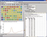
Figure 4: An array of measurements made on a single wafer using the plate reader.
Conclusion
FT-IR has been used in silicon manufacturing for many years. The tools presented here are not fabrication plant tools, but are designed for the laboratory or near-line environment. Removing the fabrication facility requirements permits the sampling system to represent an inexpensive, rapid, and reliable system for users needing such a tool. Combining long-term experience in silicon analysis, ASTM/SEMI methodology, and the plate array accessory provides an excellent nondestructive, noncontact measurement for the solar silicon industry. With application-specific software tailored for customer operation, these determinations can be performed with little knowledge of the theory of the instrument involved.
Steve Lowry is a Senior Scientist, Ross Boyle is a Senior Applications Specialist, and Mike Bradley is FT-IR Product Manager with Thermo Fisher Scientific, Madison, Wisconsin.
References
(1) SEMI organization web page: http://www.semi.org/en/About/index.htm.
(2) R. Boyle, FT-IR Measurements of Interstitial Oxygen and Substitutional Carbon in Silicon Wafers, Thermo Scientific Application Note: 50640.
(3) SEMI MF1188-1107: Test Method for Interstitial Oxygen Content By Infrared Absorption with Short Baseline.
(4) SEMI MF1391-1107: Test Method for Substitutional Atomic Carbon Content of Silicon by Infrared Absorption.
(5) B.G. Rennex, "Standard Reference Materials: Certification of a Standard Reference Material for the Determination of Interstitial Oxygen Concentration in Semiconductor Silicon by Infrared Spectrometry." NIST Spec. Publ. 260-121 (Aug. 1994).
AI Shakes Up Spectroscopy as New Tools Reveal the Secret Life of Molecules
April 14th 2025A leading-edge review led by researchers at Oak Ridge National Laboratory and MIT explores how artificial intelligence is revolutionizing the study of molecular vibrations and phonon dynamics. From infrared and Raman spectroscopy to neutron and X-ray scattering, AI is transforming how scientists interpret vibrational spectra and predict material behaviors.
Real-Time Battery Health Tracking Using Fiber-Optic Sensors
April 9th 2025A new study by researchers from Palo Alto Research Center (PARC, a Xerox Company) and LG Chem Power presents a novel method for real-time battery monitoring using embedded fiber-optic sensors. This approach enhances state-of-charge (SOC) and state-of-health (SOH) estimations, potentially improving the efficiency and lifespan of lithium-ion batteries in electric vehicles (xEVs).
New Study Provides Insights into Chiral Smectic Phases
March 31st 2025Researchers from the Institute of Nuclear Physics Polish Academy of Sciences have unveiled new insights into the molecular arrangement of the 7HH6 compound’s smectic phases using X-ray diffraction (XRD) and infrared (IR) spectroscopy.