Depth Resolution of the Raman Microscope: Optical Limitations and Sample Characteristics
The experimental determination of the depth resolution of a Raman microscope is described.

Raman microscopy has been attractive because of its ability to characterize materials on a spatial scale commensurate with optical microscopy. Typically, the lateral spatial resolution is quoted as determined by the Airy disk (1), which is 1.22λ/NA. λ is the wavelength of the illuminating light, and NA is the numerical aperture, which is equal to nsinθ, where n is the index of refraction of the medium (1.0 in the case of air) and θ is the angle subtended by the optics. However, it is interesting to this aging Raman spectroscopist that in recent years, the quoted spatial resolution of a Raman microscope has been getting smaller and smaller as more instrument manufacturers enter into the business of Raman microscopy. In fact, the spatial resolution has not been improved; one cannot redefine the laws of physics. We believe that the equations selected to "define" spatial resolution have been selected to give a smaller number. In the end, the only true way is to test the spatial resolution is to define well-controlled measurement conditions. This will be the focus of this column.

Fran Adar
For a start, we can say that the Airy disk description cannot be correct for a Raman microscope. The Airy disk assumes uniform illumination of the focusing optic, and the laser profile is anything but. In addition, in some instruments, the Gaussian laser profile is not well matched to the aperture of the focusing objective. At any rate, this article is going to concentrate on the depth resolution of the Raman microscope. Optical calculations for depth resolution of an optical microscope state that the it is proportional to λ/(NA)2. The essential point to recognize is that the spatial resolution of any Raman microscope depends upon the detection optics as well as the focusing optics. How effectively does the optical system collect the Raman signal excited in the laser focal spot, and reject the signal from the surrounding volume that is illuminated by the laser but not in focus?
Background
The essential question is how to evaluate the depth resolution experimentally. Historically, people have used a piece of a polished Si wafer for these tests. But this material was chosen more for the repeatability of any measurement of its signal rather than its appropriateness for answering the questions of depth resolution. The advantages of using silicon are that it is readily available, the optical properties of a polished surface are perfect, and the signal generated from a particular orientation using a particular laser wavelength and instrument parameters is reproducible. This last point is not to be taken lightly. Raman scattering is a "single-beam" technique, and as such there are many factors affecting the absolute magnitude of the signal. Using silicon as the test sample enables one to track the performance of an instrument and to compare signals taken under different conditions (for example, with different gratings or with the sample in a different orientation) because the signals are reproducible when a set of measurement conditions are controlled. This is a point that I have made in one of my earlier columns.
After we had determined that silicon provided a good test sample, it was realized that it could be used to test the depth resolution. However, this is where its use becomes a bit questionable. Figure 1 indicates what the problems are. Figure 1a shows the beam path for the laser focused precisely at the surface of the silicon. After the light hits the surface in focus, it will continue to penetrate the silicon as it diverges. How far it penetrates depends upon the wavelength of the laser. It turns out that in the visible part of the electromagnetic spectrum the depth of penetration is not negligible. At 633 nm, the wavelength of the HeNe laser, the light will penetrate 3 μm, but this number changes rapidly with wavelength. At 785 nm it is about 12 μm, at 532 nm it is 0.7 μm, and in the UV it can drop to 5–10 nm. What Figure 1 shows is that when the laser is focused on the sample surface, this point is reimaged on the confocal hole and entrance to the spectrograph. However, the light that diverges from the point of focus also can generate Raman light, and the path that light will take through the collection optics is shown in orange. For the point selected in the figure, the Raman light will be focused before the slit and off-center. As such, it will have little chance of passing the entrance hole. But the question is, how much is little? If we excited with 785-nm radiation, Raman light can be generated as far as 12 μm below the surface. How well is this light rejected? What about light that is 6 μm below the surface? How can this be quantitated?

Figure 1: (a) Laser beam path focused at the silicon surface, (b) microscope stage scanned in a vertical direction.
The solution was to perform a "Z scan." Figure 1b illustrates what is happening in such a measurement. In this case, the microscope stage is scanned in the vertical direction so that the surface passes through the plane of focus of the laser beam. Then you can record the intensity of the spectrum as a function of Z position. The problem with this measurement (aside from the fact that the depth of penetration is far from infinitely narrow) is that as the sample is moved away from the focal plane, a larger area is being excited by the laser beam. So the signal that is measured is a convolution of losses due to the surface not being in focus, and gains due to a larger volume being illuminated.
Is there a better way to determine the confocal properties of a Raman system? Having thought about it for a while, we decided that microscopic polymer beads might provide a solution. In this case, when the microscope stage is raised, the lateral extent from which the signal can be generated is controlled by the particle size. We will show measurements taken from Si as well as polymer beads (2 μm and 0.5 μm diameter) using the 532 nm laser beam (minimizes the depth of penetration of the laser into silicon so that the effect of the lateral illumination of the surface can be separated from the volume effect).
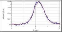
Figure 2: Depth profile of (001) Si. 532 nm excitation, 25 μm confocal hole. FWHM = 2.6 μm.
Results: Silicon
Figure 2 shows a depth profile of the silicon signal when the confocal hole was set to 25 μm. The profile was fitted to a function whose full width at half maximum (FWHM) was about 2.6 μm, which is considerably more that the depth of penetration of the light. To gain insight into what is happening, a series of confocal measurements were made on a different day. In this case, the focal plane was identified visually in the monitor, and the confocal hole was opened from 0 to 300 μm in 10-μm steps, at Z = –1, 0, 1, and 2 μm relative to the visual focus. These results are shown in Figure 3. Figure 3a shows the confocal scans displayed showing the real observed intensities; Figure 3b displays the same data, but in relative units.
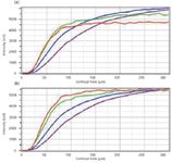
Figure 3: Confocal profiles of silicon signal recorded at Z = -1 (red), 0 (green), 1 (blue), and 2 μm (violet), with the 0-μm plane defined visually. (a) profiles of the absolute intensities; (b) profiles scaled so that the maxima for all traces were identical.
For Z = –1 and 0 μm, the signal was identical until the hole was opened to more than 55 μm. It actually is not easy to determine what the exact focal plane is by visual inspection. But, if we establish a criterion of best focus as the plane in which the confocal trace turns on most rapidly (relative to its maximum intensity, see Figure 3b) then, in this case, Z = –1 μm appears to be the better choice for focus. What is also interesting is that at Z = –1 and 0 μm, the signals are higher than at Z = 1 and 2 μm for hole sizes less than 125 μm. But for larger hole sizes, the detected signals are greater for Z = 1 and 2 μm (Figure 3a). Because we know that there cannot be a volume effect in this sample at this wavelength, this has to be due to the increased illumination area. In addition, Figure 3b shows that as the hole size is increased, it takes longer to saturate the signal, which is consistent with a larger image at the hole because the sample plane is not the laser focal plane.
Results: Polystyrene Spheres
We have recorded confocal scans (varying the height of the sample and the hole size) of polystyrene spheres with nominal diameters of 2 and 0.5 μm. Figure 4 illustrates the depth profiles of the scans of the 2-μm polystyrene spheres as the hole size is varied between 25 and 105 μm. Each of the profiles was fit to a symmetric function. The FWHM varied only between 4.7 and 5.1 μm.
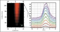
Figure 4: Confocal profiles of a 2-μm sphere of polystyrene (using the 620-cm-1 band) as the sample plane (Z) and the size of the confocal hole is varied. The left side of the figure is a full representation of the data, while the right side shows horizontal cuts through the data.
Similar measurements were made on 0.5-μm polystyrene spheres. Those depth profiles are shown in Figure 5. For a particle of such a small volume, the polystyrene signal was weaker than in the larger beads, which accounts for the noise in the depth profiles. In this case, we do observe a systematic sharpening of the profile as the confocal hole is closed. This can be visualized more readily by displaying the profiles with the same maxima, as seen in Figure 5b.
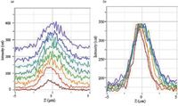
Figure 5: Depth profiles of 0.2-μm polystyrene sphere recorded with the confocal hole set to 200, 175, 150, 125, 100, 75, 50, and 25 μm (top to bottom). (a) Profiles shown with absolute intensities, displaced vertically for viewing; (b) profiles overlaid with same min/max intensity to visualize the change in profile width.
The right-hand part of the figure shows that the intensity starts to appear at the same Z position (at the top of the sphere), but when the hole is enlarged, the intensity drop-off at the bottom of the sphere is delayed, resulting in a larger profile, and an apparent displacement of the peak position.
These profiles were also fitted, resulting in Table I.
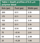
Table I: Depth profiles of 0.5-μm polymer bead
Results: Silicon Under 0.-5 -μm Polystyrene Sphere
These measurements held a surprise for us. The 0.-5 -μm polystyrene spheres had been deposited on Si (whereas the 2-μm spheres were on Al). So we were able to plot the depth profiles of silicon under a sphere and compare them to profiles of silicon. Figure 6 shows the depth profiles under the bead.
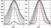
Figure 6: Depth profiles of silicon signal when measured under a 0.5-μm polystyrene sphere. Confocal hole (from top to bottom) was 200 to 25 μm in 25-μm increments. Left: profiles in absolute intensity; right: profiles displayed with the same min to max.
Figure 7 shows the depth profiles, with a 25-μm hole, of bare silicon versus silicon under a bead. Note that these profiles were measured sequentially on the same day under identical conditions. We observe several things in this measurement: The signal under a bead was higher than on the bare silicon, and the FWHM was tighter under the bead.
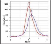
Figure 7: Sequential measurements of depth profile on silicon, measuring through/under a 0.5-μm polystyrene bead (red) versus measuring on bare silicon (purple). The confocal hole was 25 μm in both cases.
The conclusion to be drawn is that the bead is acting as a solid immersion lens that increases the effective NA of the focusing, which, in turn, decreases the spot size, and increases the collection efficiency!
Remarks on Subsurface Measurements
Because of the confocal nature of Raman measurements there are a number of applications that can be addressed uniquely with this technology. They include diffusion of one chemical species into or through another, and the sharpness of an embedded interface. Once anyone tries these measurements, it becomes clear that below-surface confocality is compromised with the objectives that usually are used. This was recognized quite early in a technical note (2) but followed up on in more detail in publications from a number of laboratories (3). In particular, these publications deal with the effect of spherical aberrations, introduced when using dry (metallurgical) objectives to study materials below the surface. These effects have not been discussed in this column, but it is clear that if one is monitoring a subsurface interface, one must include consideration of both effects. The best objective for the sample must be selected, and a confocal hole consistent with the desired spatial resolution must be used.
Conclusions
The experimental determination of the confocal depth from which Raman signal is collected is determined by instrumental parameters, sample parameters, and, sometimes, interactions between the sample and the optics. While a sample like silicon is ideal for reproducibility, it is not ideal for defining depth resolution because as the sample is defocused, a larger illuminated area provides a larger signal. By making measurements at 532 nm, where the depth of penetration of the light is less than a micrometer, we were able to document this effect. When the confocal hole was 200 μm, the FWHM of the depth profile was greater than 6 μm, but at 25 μm the FWHM was not much greater than 2 μm, which was close to the number recorded for the 0.5-μm sphere of polystyrene. Because the 0.5-μm spheres of polystyrene were mounted on silicon, it also was possible to compare silicon depth profiles measured on bare silicon and silicon under a sphere; under the sphere, the silicon signal was stronger and the depth profile was sharper, leading to the conclusion that the polymer sphere is functioning as a solid immersion lens. The bottom line is that confocal measurements on a Raman microscope must be made with an understanding of the optical behavior of both the instrument and the sample, and their possible interactions. As a follow-up to this discussion, my next column will consider the role of sample characteristics in the choice of sampling optics and the consequential spatial resolution. In particular, we will consider the interesting situation in which one needs to minimize spatial resolution to achieve a macroscopic signal representing the true sample average.
Fran Adar is the Worldwide Raman Applications Manager for Horiba Jobin Yvon (Edison, NJ). She can be reached by email at fran.adar@horiba.com
References
(1) M. Born and E. Wolf, Principle of Optics: Electromagnetic Theory of Propagation, Interference and Diffraction of Light, 7th Edition (Cambridge University Press, Cambridge, UK, 1999).
(2) "Raman chemical depth profiling with automated Z focus" (ISA Technical Note R-27, June 1998).
(3) N. Everall et al., Appl. Spectrosc. 61, 251 (2007).

A Proposal for the Origin of the Near-Ubiquitous Fluorescence in Raman Spectra
February 14th 2025In this column, I describe what I believe may be the origin of this fluorescence emission and support my conjecture with some measurements of polycyclic aromatic hydrocarbons (PAHs). Understanding the origin of these interfering backgrounds may enable you to design experiments with less interference, avoid the laser illuminations that make things worse, or both.
Raman Microscopy for Characterizing Defects in SiC
January 2nd 2025Because there is a different Raman signature for each of the polymorphs as well as the contaminants, Raman microscopy is an ideal tool for analyzing the structure of these materials as well as identifying possible contaminants that would also interfere with performance.