High-Speed TERS Imaging: The Latest Achievements in nano-Raman Spectroscopy
Special Issues
This article presents developments in tip-enhanced Raman spectroscopy (TERS) that make possible nanoscale imaging of chemical and physical properties of graphene and other carbon species: Innovative integration of technologies brings high-throughput optics and high-resolution scanning for high-speed imaging without interferences between the techniques.
This article presents developments in tip-enhanced Raman spectroscopy (TERS) that make possible nanoscale imaging of chemical and physical properties of graphene and other carbon species: Innovative integration of technologies brings high-throughput optics and high-resolution scanning for high-speed imaging without interferences between the techniques. Advances in near-field optical probes now provide reliable nanoscale spectroscopy solutions for academic and industrial researchers.
Raman spectroscopy is a well-known technique to study carbon species. It provides a very specific signature for the two crystal configurations: diamond (cubic or octahedral) and graphite (hexagonal).
Because Raman microspectroscopy is an optical technique, its spatial resolution is limited by the laws of diffraction: As a rule of thumb, the spatial resolution of the technique is about half the wavelength of the exciting laser wavelength. This value depends on several factors besides the excitation wavelength, including the numerical aperture of the objective lens used; however, this approximation is convenient and easy to understand for the purpose of this discussion. With a red laser excitation, this is on the order of 300 nm.
Graphene flakes or coatings can be made quite large; however, other species of interest like single-wall carbon nanotubes (SWCNT) are typically in a diameter range of 1–3 nm, or two orders of magnitude smaller than the spatial resolution of the technique.
Raman spectroscopy brings chemical contrast for these species, and allows the determination of the diameter of a single wall carbon nanotube, or the number of layers in a multilayer graphene sample from the features present in the spectrum. Radial breathing mode frequency position is a good indicator of SWCNT diameter or the ratio and bandwidth of the G and two-dimensional (2D) bands in graphene are good indicators of the number of layers. However, the samples measured are generally not resolved spatially.
In contrast, scanning probe microscopy (SPM) and, in particular, the more popular technique atomic force microscopy (AFM) allow such materials to resolve spatially and provide even atomic-level resolution. Atomic resolution imaging of highly ordered pyrolytic graphite (HOPG) is a typical test for SPM calibration, using scanning tunneling mode (STM). The technique consists of scanning a very sharp probe over a sample and tracking the Z axis position via a feedback mechanism that depends on the mode used, to generate a topographic image. In STM, the feedback is done based on tunneling current intensity, and in AFM, a constant force is maintained between the probe and the sample by tracking the deflection of a laser on the back of a cantilever that holds the sharp probe. The cantilever bends according to its known mechanical properties that depend on size, shape, and material.
Beside topography, AFM can be used in a multitude of modes to obtain various physical properties. Looking at the way the probe interacts with the sample, it is possible to determine elasticity and plasticity of a material. Tracking the torsion of the level as it is scanned (lateral force) gives information about friction. Driving a current through a conductive probe, it is possible to obtain various electrical properties such as conductance, capacitance, and resistivity; surface potential is also determined by scanning above the surface. Using a magnetized probe, magnetic studies can be performed at various heights from the surface.
SPM and, in particular, AFM are very versatile techniques to image a multitude of physical properties, however, neither technique provides chemical specificity (except in the case of the use of functionalized probes designed for very specific chemical bonding).
The interest for combining the two techniques is obvious: Obtaining physical properties and chemical specificity of the same location, ideally simultaneously, without having to move the sample or find the location of interest each time is a huge time saver when studying nanomaterials.
The combination of the two techniques is in itself interesting, but furthermore reducing the spatial resolution gap between the two techniques is of the highest interest. This is where tip-enhanced Raman spectroscopy (TERS) comes into play.
TERS takes advantage of the enhancement of several orders of magnitude observed in techniques like surface-enhanced Raman spectroscopy (SERS), confining this enhancement at the tip of a specially crafted probe that acts as a plasmonic antenna. The result of this confined resonance is an extremely localized enhancement of the Raman signal in the very close vicinity of the tip of the probe, generally no further than 10 nm. A laser beam matching the probe's plasmonic excitation range is focused on the probe to produce the local enhancement. The focused laser beam is of course following the same diffraction rules mentioned above, and illuminates a field much larger than the probe tip radius, potentially exciting a far-field (diffraction limited) Raman signal, while the enhanced signal is localized just under the probe generating the near-field Raman signal. The ratio of the volumes involved in each case is also several orders of magnitude, so the ability to detect the near-field Raman signal is extremely dependent on the probe quality and its enhancement efficiency.
SWCNTs have been studied in the past with TERS, most often performing line scans (1) and a few produced images (2).
The novelty presented here and demonstrated in the experimental measurement of graphene oxide and single-wall carbon nanotube samples is in the combination of the techniques into an instrument in such an efficient manner that it is possible to obtain reliable enhancement and stable alignment to perform TERS imaging with very short acquisition times, which in turns frees the technique from the need to subtract far-field from near field and from potential drift issues inherent to the SPM technology.
Experimental
The experimental setup consists of a nano-Raman integrated system from Horiba Scientific and AIST-NT Inc. A SmartSPM scanning probe microscope (AIST-NT Inc.) with an Omegascope microscope was used for top-down and oblique illumination and collection. The microscope is integrated with a Horiba XploRA Plus Raman microspectrometer (or it can eventually also be fitted with a Horiba Labram HR Evolution spectrometer for added functionalities). In this configuration, the spectrometer was fitted with an electron-multiplying charge-coupled device (CCD) detector for fast data acquisition.
In this work, different samples were prepared. The first set of images generated consists of colocalized confocal Raman and AFM imaging of graphene flakes. The sample is mechanically exfoliated graphene deposited on a silicon substrate using the widely referenced transparent adhesive tape method. In this case, a 532-nm laser was used for Raman spectroscopy, with a power of 25 mW at the sample. Acquisition time for the image shown is about 7 ms per point. The area measured is 35 µm × 35 µm.
The second sample was prepared by dispersion of a graphene oxide and carbon nanotube mixture from solution spin-coated on a flame-annealed 5 mm × 5 mm gold substrate. Spin-coat time and solution concentration were adjusted to obtain a distribution of about one or two tubes and one or two graphene oxide flakes per square micrometer, so as to easily find an area of interest while avoiding aggregation of nanotubes. This second sample was measured with AFM first to verify the proper distribution of the two carbon species, and then it was imaged with TERS. The laser wavelength used was 638 nm. The laser output power is typically 24 mW, but only a few hundred microwatts to about 6 mW were used in this case.
In performing AFM-Raman imaging or TERS, a critical step consists of making sure the Raman laser is properly aligned with the probe. In AFM-Raman imaging, an offset in the order of the spatial resolution of the Raman technique is acceptable, but it is much less forgiving when performing TERS measurements. For this purpose, the Raman laser is aligned using a piezo-driven objective scanner, with closed-loop feedback, similar to the scanning probe microscope sample scanner. This device ensures the long term stability of the alignment. Since it displaces the objective lens only, it does not introduce any additional optical component, guaranteeing maximum throughput, and since it is effectively moving the last piece of optic before the sample, the beam pathlength is minimized for best stability.
Another notable feature of the setup is the use of an infrared diode for AFM feedback. Most SPM systems use a diode in the red or near-infrared (NIR) range, potentially interfering with the collection of the Raman signal in those spectral ranges. Avoiding this range is especially critical for AFM-TERS, using an AFM cantilever, as the most stable probes today are made out of gold whose plasmon resonance frequency is in the red region. Using an infrared feedback diode ensures there is no interference with the optical spectroscopy system. Furthermore, the AFM diode is not visible in the video image and does not tend to excite fluorescence in the sample, allowing artifact-free Raman measurements.
The dual microscope setup brings a few advantages: It allows top down measurements, which makes simultaneous and colocalized measurement of AFM images and spontaneous Raman hyperspectral images possible, with high spatial resolution. The top-down approach is best for high spatial resolution on opaque samples in spontaneous Raman measurement mode because the laser can be tightly focused with a high numerical aperture (NA) objective lens (0.7 NA in our case when simultaneous AFM and Raman measurements are made, and up to 1.4 NA with oil immersion objectives when the AFM probe is removed for Raman measurements only).
The oblique (or side) illumination scheme is not ideal for spontaneous Raman measurement as the laser spot is focused at a 60° angle and, therefore, is not Gaussian but elliptical. Spatial resolution is degraded, but this is the preferred mode of illumination for tip-enhanced Raman measurements because it allows better illumination of the apex of the probe, while providing proper alignment of the electromagnetic field of the incident laser beam with the axis of the plasmonic probe without the need for further polarization conditioning of the beam.
It has been shown in simulation that this illumination scheme also brings the highest surface plasmon resonance enhancement of the Raman signal and that it is then localized directly under the apex of the probe (3), as opposed to the side when polarization orientation is not optimized. This confinement of the Raman enhancement below the probe apex, providing the probe has a high enhancement contrast, is what brings spatial resolution of the near-field Raman signal down to about 10 nm, well below the actual probe apex radius, which is typically in the order of 30 nm.
The probes used are commercially available probes manufactured by Horiba and made from etched gold wire following a process adapted from the original publication by Bin Ren and colleagues (4) and improved by the Laboratoire de Physique des Interfaces et des Couches Minces (LPICM) laboratory of the Ecole Polytechnique in France. The probes are mounted on a tuning fork for this experiment.
TERS imaging has been considered to be very complex because of the many factors that may affect the measurement. The novelty in the equipment primarily consists in the use of efficient, reliable probes developed in collaboration with academic researchers, in the optimization of the optical path and alignment technology to reduce drift, and in the integrated control of the different hardware components to improve data acquisition speed, which in turn reduces potential drift issues.
In the setup described, the measurement time is typically 5–100 ms. This is possible thanks to the use of the electron multiplying charge coupled device (EMCCD) detector that allows detection of signals below the read noise of the device. Such a detector is very popular in fluorescence microscopy for this capability; however, in spectroscopy it has a few trade-offs and is essentially useful to accelerate acquisition. EMCCD technology adds a gain factor called electron-multiplier before the electrical signal is converted into a digital signal through the analog-to-digital converter (ADC). This, in effect, allows the detection of signals below the read noise, which is the noise produced by the ADC while converting. However, this also has the effect of dramatically reducing dynamic range because any signal above the read noise is enhanced to levels bringing it closer to the saturation level of the ADC. This gain process does not effectively bring any advantage when the signal is already above the read noise level. Considering a Raman signal with a signal to noise ratio of 100:1 obtained in 1 s, if we decrease integration time to such a level that the signal is below the read noise, in our case 10 ms for example, the electron-multiplier gain can now bring this signal above the read noise level and enhance it to regain a readable spectrum with enough contrast to extract information about the bands of interest and generate an image rendering based on this information.
However, using the electron-multiplier gain does not produce high quality spectra. Longer acquisition times or the accumulation of multiple spectra is usually necessary to obtain data that can be used for precise spectral analysis. The technique, however, can image and locate areas of interest quickly, which can then be investigated further.
Results and Discussion
The first measurements consist of the analysis of graphene flakes of different size and thickness. Figure 1 shows a topography image of the sample, which gives information on the graphene flake thickness. Even though the topography image can help determine the presence of single-layer or multiple-layer graphene, the roughness of the substrate itself, which can be much larger than the single atomic step of carbon, can understandably interfere with this measurement.
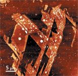
Figure 1: AFM topography of a set of graphene flakes of different thickness.
Figure 2 is the surface potential image of the sample, also known as Kelvin probe force microscopy (KPFM), and provides information about the electronic state of the surface of the sample.
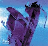
Figure 2: Surface potential difference image of the graphene flake sample. This technique, also referenced to as Kelvin probe microscopy, provides information about the electronic state on the surface.
Figure 3 shows a false color composite Raman image of the sample generated from classical least squares deconvolution of the Raman hyperspectral data cube. The silicon substrate is shown in grey, single-layer graphene is shown in purple, two-layer graphene is shown in blue, three-layer graphene is shown in green, amorphous carbon is shown in yellow on a couple spots (this is believed to be from over-exposure with the Raman laser), and defective graphene is shown in orange, which is primarily concentrated on the edges of the flakes.
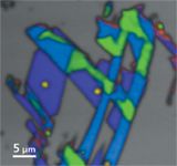
Figure 3: False color image generated from classical least square deconvolution of the Raman hyperspectral image. The silicon substrate is shown in gray, single-layer graphene is purple, two-layer graphene is blue, three-layer-graphene is green, amorphous carbon is yellow, and defective graphene is orange, primarily concentrated on the edges of the flakes.
In this example, it can be seen that the Raman image is of lower spatial resolution than the AFM images even though the number of data points is equivalent as the topography and Raman images were generated simultaneously. The KPFM image can be generated in one pass, but it is most often generated in two passes to avoid cross-talk, so this image was generated separately.
It is undeniable in these images that complementary information is obtained, demonstrating the usefulness of the technique. The topography can be correlated closely to the Raman spectral information, which provides clear confirmation of the graphene flake thickness.
Raman spectroscopy provides more detailed information on the chemical structure of the graphene and especially the presence of defects, which are more commonly found on the edges of the flakes. This can easily be explained by the fact that the ordered hexagonal lattice is indeed disrupted at the edge.
The ability to generate multiple images simultaneously is common in scanning probe microscopy where electrical signals are measured, however, acquiring Raman spectra calls for a very different approach and the use of a CCD detector, which tends to be much slower. The ability of the equipment to perform both simultaneously ensures that the data obtained effectively come from the same location.
Because we are using a sample scanner, effectively moving the sample in all three dimensions (X, Y, and Z) the sample is moved to track the cantilever position, as opposed to adjusting the cantilever position to track the sample. This has an added advantage because of the fact that the Raman laser, which is also aligned on the probe, remains in focus on the sample at all times, no matter what the height of the topography is, essentially acting as a real-time autofocus. This is not evident in the sample measured in this work, but becomes critical when looking at samples with topography in the several micrometer range: Because of the confocal nature of the system, the depth of field is only on the order of a micrometer, and without tracking the sample position, only a thin Z slice of the sample would be measured properly.
The next experiment demonstrates Raman imaging at high speed with nanoscale resolution.
The TERS image in Figure 4 is 200 × 200 points mapped over a 2 µm × 2 µm area and was obtained with 12 ms acquisition time per spectrum, yielding 40,000 points in about 8 min. It has been deconvoluted with a classical least squares method to extract the three compo nents of interest: the graphene oxide, the carbon nanotubes, and the background signatures, shown in false colors in red, green, and black, respectively.
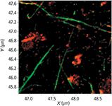
Figure 4: Image of carbon nanotubes (green) and graphene oxide (red) on gold substrate obtained in tuning fork mode. This 200 à 200 point, 2 à 2 µm image was obtained in 8 min with spatial resolution of 10 nm.
This method yields the most contrast when the goal is to differentiate the different carbon species, but misses the information contained in the specific bands of interest. In particular, the D band (around 1330 cm-1) is typically associated with disorder in the hexagonal carbon structure.
Figure 5 shows the individual images generated by rendering intensity of the specific carbon bands. The D band is shown in red, the G band is shown in green, and the 2D band is shown in blue.

Figure 5: Images of the D band (red), G band (green), and 2D band (blue) of the graphene oxide and carbon nanotubes sample. The nanotubes show strong typical G and 2D bands while graphene oxide shows no 2D band but high disorder (D band). Some nanotubes show higher disorder than others in the presence of a D band as well.
Graphene oxide is highly disordered and shows strong D band and G band typical of the graphitic structure. Carbon nanotubes show strong G and 2D bands as is typical, but also show some presence of a D band in some areas, indicating the presence of defects in the tube structure.
Figure 6 shows the overlay of all three colors, bringing graphene oxide in yellow (mixture of red and green) and carbon nanotubes mostly in various shades of blue indicative of the defective structure.
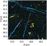
Figure 6: Overlay of the three images from Figure 2.
In Figure 7, a close-up image was generated. It is 50 × 50 points, 2-nm steps, and was obtained in 40 s. Figure 8 shows the corresponding spectra extracted by classical least squares deconvolution of the image in Figure 7.
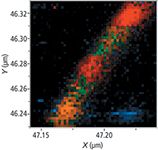
Figure 7: Close-up image of a nanotube. The image is 100 Ã 100 nm with 2-nm steps (50 Ã 50 points, obtained in 40 s).
This image is a good illustration of the variability of the nanotube chemical structure at the nanoscale which is impossible to resolve with standard confocal Raman imaging, and which cannot be extracted by typical SPM techniques. In these spectra, we observe a range in level of disorder in the carbon material from the red spectrum (low disorder, low intensity of D band) to green to orange (higher level of disorder, highest intensity of D band).
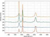
Figure 8: Reference spectra for classical least squares deconvolution of the image in Figure 7.
Conclusions
This work does not pretend to expose novel science or understanding of AFM-Raman and TERS, but aims at demonstrating the current capabilities available today. Imaging carbon nanotubes with TERS has been done before, however, there are very few publications demonstrating this capability on a strictly commercial instrument. The leading groups in TERS have demonstrated the capabilities of the technique for several years now, yet even though many of the setups used are built from commercially available systems, almost all have been modified for the purpose of developing the technique.
Researchers wanting to approach this technique today are faced with the need to account for many subtle, but important modifications to get results.
In this work, we presented the capabilities of a strictly commercial instrument designed for purpose. Evidently, one of the key factors in successful TERS is the availability of suitable and efficient probes. With the development of its own probe manufacturing in collaboration with academia, a complete solution for TERS is now commercially available. Furthermore, many of the limitations that make AFM-TERS difficult have been removed, and the platform is ready to use such probes when they become available, without the risk of optical interference.
In the past, TERS was not a technique reserved for the faint-hearted; this work shows that it is now easier than ever to get results quickly and reliably. Many years of experience have been put into perfecting the instrumentation. Now, this experience is available and application development is the focus of research.
E. Leroy, R. Lewandowska, O. Lancry, and J. Schreiber are with Horiba Scientific in Palaiseau, France. A. Krayev and S. Saunin are with AIST-NT Inc., in Novato, California. Direct correspondence to: Emmanuel.leroy@horiba.com
References
(1) G. Picardi, M. Chaigneau, and R. Ossikovski, Chem. Phys.Lett. 469, 161 (2009).
(2) L.G. Cançado, A. Hartschuh, and L. Novotny. J. Raman Spectrosc. 40(10), 1420–1426 (2009).
(3) A. Downes, J. Phys. Chem. B 110, 6692 (2006).
(4) B. Ren, G. Picardi, and B. Pettinger, Rev. Sci. Instrum. 75, 837 (2004).

AI-Powered SERS Spectroscopy Breakthrough Boosts Safety of Medicinal Food Products
April 16th 2025A new deep learning-enhanced spectroscopic platform—SERSome—developed by researchers in China and Finland, identifies medicinal and edible homologs (MEHs) with 98% accuracy. This innovation could revolutionize safety and quality control in the growing MEH market.
New Raman Spectroscopy Method Enhances Real-Time Monitoring Across Fermentation Processes
April 15th 2025Researchers at Delft University of Technology have developed a novel method using single compound spectra to enhance the transferability and accuracy of Raman spectroscopy models for real-time fermentation monitoring.
Nanometer-Scale Studies Using Tip Enhanced Raman Spectroscopy
February 8th 2013Volker Deckert, the winner of the 2013 Charles Mann Award, is advancing the use of tip enhanced Raman spectroscopy (TERS) to push the lateral resolution of vibrational spectroscopy well below the Abbe limit, to achieve single-molecule sensitivity. Because the tip can be moved with sub-nanometer precision, structural information with unmatched spatial resolution can be achieved without the need of specific labels.