Key Elements of Confocal Raman Microscopy for High-Resolution Imaging
Special Issues
The sensitivity of a high-resolution Raman imaging system is crucial to the quality of the acquired information.
The sensitivity of a high-resolution Raman imaging system is crucial to the quality of the acquired information. The spectral and spatial resolutions are among the primary factors that influence the obtainable results. The limits of resolution are defined theoretically by the laws of physics, but are experimentally determined by the instrument parameters. In this article, the theoretical background and the possibilities in practical applications are discussed.
Confocal Raman microscopes are the instruments of choice for many Raman measurements in a wide variety of applications ranging from geosciences (1–3), biology (4–6), nanocarbon materials (7–9) to pharmaceutical compounds (10,11), just to name a few. This article sheds light on the possibilities and, in part, the origins in terms of spectral and spatial resolution for confocal Raman systems in general.
Spectral Resolution
Any confocal Raman system will have a spectral resolution which is mainly determined by the following parameters:
- the focal length of the spectrometer (the longer the focal length, the higher the spectral resolution)
- the grating (the higher the groove density, the higher the spectral resolution)
- the pixel size on the charge-coupled device (CCD) camera (the smaller the pixels, the higher the spectral resolution)
- the entrance slit or pinhole (the smaller the slit or pinhole the higher the spectral resolution)
- the line shape preservation (equals imaging quality) of the spectrometer.
In some cases, one of the parameters can put limitations on the spectral resolution. If, for example, the projection of the pinhole onto the CCD is already large compared to the pixel size on the CCD camera, then a further reduction of pixel size will not increase the spectral resolution.
Please note that the microscope components such as the objective used for collection of the signal should not influence the spectral resolution if the entrance slit or pinhole is the limiting element. This is preferential with confocal Raman microscopes.
The determination of the spectral resolution is often a point of debate. First, one should clearly differentiate the spectral resolution from the sensitivity of the system to detect shifts of individual peaks. Relative peak shifts can be detected with a much higher accuracy using fitting algorithms as has been demonstrated with a sensitivity down to 0.02 rel. 1/cm standard deviation of the peak shift of a Si peak (12). The maximum achievable fit accuracy depends heavily on the number of detected photons and the width of the peak that is fitted. This shift analysis is especially relevant for examining stress within a sample, but may not be taken as a measurement for the spectral resolution.
The spectral resolution, which determines how the system can measure (that is, full width at half maximum [FWHM] of a narrow peak or how well overlapping peaks can be differentiated), needs to be addressed separately from the peak shift sensitivity. There are various ways to state the spectral resolution, and some of the most common ones are outlined below.
Pixel Resolution
The pixel resolution is the difference in wavenumbers when moving from one pixel on the CCD camera to the next and is independent of factors such as slit width or peak width of the detected peak. This can only be seen as the true resolution limit if the pixel size and not the size of the entrance slit or pinhole is the limiting factor. For example, if the image of the slit or pinhole on the CCD camera is 100 µm in diameter and the pixel size on the CCD camera is 26 µm, then the resolution would be significantly worse than the distance (in wavenumbers) between two pixels. Since wavenumbers are measured in reciprocal space, it also needs to be noted that the pixel resolution will differ depending on the spectral position where it is determined. The resolution close to the Rayleigh line can, in this way, differ by almost a factor of two from the pixel resolution near 3500 rel. 1/cm in the case of 532-nm excitation.
Two-Pixel Criterion
For this criterion two times the pixel resolution is taken. The logic behind this is that to discriminate two neighboring peaks one needs to have one pixel on one peak, one in the minimum between the peaks, and a third one on the next peak. This criterion is analogous to the Nyquist theorem in signal processing. The same limitations as outlined for the pixel resolution criterion apply in this case.
Full Width at Half Maximum of Atomic Emission Lines
Atomic emission lines are typically much narrower than any Raman line. Their narrow width makes them a good probe to check the resolution. Figure 1 shows an atomic emission line of mercury near 579.07 nm. The x-axis is given in units of rel. 1/cm assuming a 532.00-nm excitation laser. The spectrum was recorded using a mercury and argon calibration lamp coupled via a 10-µm core diameter multimode fiber to a UHTS300 spectrograph (WITec GmbH) equipped with both 1800- and 2400 grooves/mm gratings (BLZ at 500 nm) and a Newton electron multiplying charge coupled device (EMCCD) camera with a pixel size of 16 µm. The integration time was 0.1 and 0.24 s, respectively, for the spectra. The FWHM derived through this approach is a good measure of the resolution, but care must be taken to ensure that enough points are available within the curve to ensure a good fit to the curve.
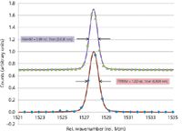
Figure 1: Spectra of the mercury atomic emission line at 579.066 nm plotted as a function of wavenumber assuming a 532.00-nm excitation. The red line is the fitted curve (pseudo voight function) and the blue diamonds are the measured data points for the 1800-grooves/mm grating. The green triangles and the purple curve show the results obtained using the 2400-grooves/mm grating.
Measurement of Peak Resolution on Known Reference Samples
There are a few samples that are established standards to demonstrate spectral resolution. The most prominent is probably CCl4. Figure 2 shows two spectra of this substance recorded with different spectral resolutions. It can clearly be seen, that the peaks are nicely separated in the red spectrum whereas the separation is not as clear for the purple spectrum.
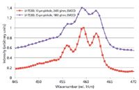
Figure 2: Raman spectrum of CCl4 with 532-nm excitation at different spectral resolutions.
Therefore, spectral resolution can be defined in many different ways and, thus, it is advisable to specify exactly how a spectral resolution was or should be determined. Comparing actual measurement results under identical measurement conditions is certainly one of the best ways to illustrate this. It should also be noted that with few exceptions the natural linewidths of Raman lines are typically larger than 3 rel. 1/cm. Taking the Nyquist criterion into consideration, a resolution in the range of 1 rel. 1/cm should be sufficient for the majority of samples.
Spatial Resolution
When considering the spatial resolution of a confocal Raman microscope one may distinguish between the lateral (x and y) resolution and the depth resolution. However, in either case, it is possible that the limitations arise because of one of the five following points:
- basic physics (that is, diffraction limit)
- limited positioning accuracy of the mechanical components used
- limitations because of the optical components used in the beam path (that is, beam distortion)
- nondiffraction limited sample illumination
- pixel resolution of the image acquired.
In terms of the positioning system, it is important to differentiate the single step accuracy of a stepper motor, the positioning reproducibility, and linearity. The reproducibility and linearity are the key factors for an imaging system since this allows a line by line imaging. If, for example, a straight line is imaged, then this line will only be imaged with the accuracy of the positioning reproducibility even though the step size might be much smaller. Figure 3 illustrates this effect with Figure 3a showing insufficient positioning reproducibility and Figure 3b showing sufficiently high positioning reproducibility.

Figure 3: A straight line imaged with (a) insufficient positioning reproducibility and (b) sufficient positioning reproducibility.
The necessary positioning reproducibility should therefore be several factors better than the smallest imaged object, or if the system should allow the best physically possible resolution, several factors (that is, 10×) better than the diffraction limit.
Using high-quality components and positioning systems should allow imaging approaching the limits of physics.
Lateral Resolution
Based on the diffraction theory of Ernst Karl Abbe, Lord Rayleigh defined the diffraction limit in 1896. Rayleigh thereby quantified the minimal distance at which two point light sources can be identified. In this case, one of the sources is located at exactly the distance of the first minimum of the Airy function (point spread function) of the other one. This distance (dlim) can be expressed as a function of the wavelength emitted (λ) and the numerical aperture (NA) of the objective used as:

The equation 1.22 λ/NA is often also found in this context, but this describes the distance between the two first minima of the Airy function and not the diffraction limit as described by Lord Rayleigh. Using the definitions of the Airy function the resolution can be easily derived by how much the intensity between the two emitting points has to decrease according to the Rayleigh criterion. Please note that the distance is different for other criteria of diffraction such as the Abbe criterion or the Sparrow criterion.
To derive the resolution of a microscope using either of those criteria it would be necessary to have a variety of very small, well scattering objects (small compared to the size of the Airy disk; for example individual TiO2 particles) at varying distances. Following high-resolution Raman imaging, one would then have to analyze the signal intensities and based on the detectable distances between the spots one would have to derive the resolution.
An easier way to determine the lateral resolution power of a system uses the FWHM of small objects. Based on the Airy function the relation between the FWHM of the light emitted from an object and the diffraction limited distance (dlim) is

Because the measured signal is always a convolution between the object size, the emission characteristics, and the system function, the objects measured in such experiments also have to be small compared to the Airy disk. Mathematically speaking, the object's size should approach a delta function for the convolution. Such small objects naturally have only limited material which scatters and thus one may expect small Raman signals emitted by them. Carbon nanotubes (CNTs) on the contrary show a large Raman signal while being very small in diameter (typically ranging from subnanometer to a few nanometer range) and comparatively long (up to a few micrometers typically). These samples are thus the ideal probes to check the lateral resolution of a confocal Raman microscope. For a 532 nm excitation laser and an objective with an numerical aperture (NA) of 0.9 one should therefore be able to obtain a FWHM across CNTs of about 301 nm.
Figure 4a shows the integrated intensity of the G-band on a sample of CNTs on a Si substrate. The scan range was 1.5 µm × 1.5 µm with 50 × 50 points and an integration time of 23 ms per point was used. An alpha300R system (WITec GmbH) was used for the measurement in combination with a fiber-coupled, frequency-doubled Nd:YAG laser (532 nm emission), a Zeiss 100× NA 0.9 objective, and a 50-µm multimode fiber acting as the pinhole for confocal microscopy. For this microscope and objective this corresponds to a projected pinhole size of 500 nm in the focal plane. The spectrometer used was a UHTS300 (WITec GmbH) with a 600-grooves/mm grating (BLZ at 500 nm) combined with a back-illuminated CCD camera.

Figure 4: Integrated intensity of the G-band of a carbon nanotube with (a) the cross section position marked in red and (b) the cross-sectional intensity along this line. The lateral resolution of the microscope system can be characterized by the FWHM and is about 272 nm.
The red line in Figure 4a indicates where the cross section shown in Figure 4b was extracted from. It can clearly be seen that the FWHM is even narrower than the predicted minimum.
The theory of confocal microscopy (for example, see reference 13) shows that the achievable resolution can further be decreased by a maximum of 1/√2. In confocal Raman microscopy this fact is rarely used to its limit, because it requires a strong reduction of the pinhole diameter, which in turn reduces the throughput.
Depth Resolution
Depth resolution is the best proof of the confocality of a system. The instrument design has a key influence on the achievable resolution, but the pinhole or slit as well as the way the sample is illuminated also play a crucial role for the depth resolution. Therefore, these points are outlined below before the physical limit of the depth resolution is discussed.
Pinhole or Slit
The pinhole plays a crucial role for the depth resolution in confocal microscopy. However, the physical size of the pinhole (Pphysical) cannot easily be compared between different instruments. In image generation using two simple lenses, the focal length of both lenses contributes to the ratio between the object and the image size. This of course also holds true for a microscope. Here, we have the magnification of the objective (MObjective), which is calculated for a certain focal length of the tube or telan lens (fTube, Objective). This focal length ranges for commercial microscopes from 164.5 mm for Zeiss objectives up to 200 mm for Leica or Nikon objectives. The magnification printed on the objective is only correct if the objective is designed for the tube focal length of the microscope. To have a comparable value for the pinhole size one should therefore calculate the projected pinhole size (Pproj) as follows:
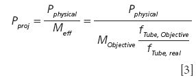
The same calculation also applies if a slit is used as a pinhole. For the following considerations, we will use the projected pinhole instead of the physical pinhole size.
The influence of the projected pinhole size is illustrated in Figure 5. Here, a point illumination of a small area with an objective with a relatively high NA value is assumed. The collection diameter of the objective is assumed to be larger than the area shown and, thus, this is assumed not to be the limiting factor here.
If the sample is transparent enough, the light will propagate further through the sample beyond the focal plane as shown by the illumination cone in Figure 5. This light can excite out-of-focus molecules, which can then emit light (Rayleigh, fluorescence, Raman, and so on) in turn. This emission is isotropic, so part of the light will find its way through the position of the projected pinhole in the focal plane and, thus, also through the physical pinhole. When comparing Figures 5a and 5b, it is apparent that a large pinhole allows a much higher amount of out of focus light to be detected. Therefore, a larger pinhole as well as a slit can never achieve the same suppression of out of focus light compared to a small pinhole.
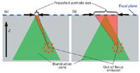
Figure 5: The light collected from an out of focus emitter through the projected pinhole and thus the physical pinhole for the case of (a) a small pinhole and (b) a large pinhole or slit.
Sample Illumination
In the last section it was shown that part of the emission from out-of-focus material will always pass through the pinhole and that the contribution of this emission to the detected signal is highly dependent on the pinhole size. The intensity of the excitation light at such an out-of-focus position is, in addition, directly proportional to the emitted light. This intensity is decreasing with an increasing distance of the point from the focal plane. The strength of this decrease, however, is heavily dependent on the way the sample is illuminated and can best be compared by taking the power density (power or area) into consideration. Given a fixed illumination power, one can simply take the increase in the illuminated area as a function of depth into consideration. The numerical aperture of the objective is essential in this consideration. The higher the numerical aperture, the faster the increase of the area as a function of depth and, thus, the faster the decrease of the power density as a function of depth. In addition to the numerical aperture, the way the sample is illuminated plays a key role. Global illumination shows the smallest decrease as a function of depth. Line illumination shows a faster decrease and point illumination gives the fastest decrease of the laser power density as a function of depth (see Figure 6). For the example shown, a point focus of 0.5 µm diameter, a line focus of 1 µm × 100 µm, and a global illumination of 100 µm diameter was used. The NA value used for the calculations was 0.9. For this approximation, a truncated cone was used as the geometry of the point and global illumination and a truncated pyramid were used for the line illumination.
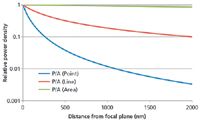
Figure 6: Relative laser power density as a function of distance from the focal plane.
Real-world samples have additional absorption of the laser power as a function of depth, but this would affect all three curves similarly.
Thus, when comparing point illumination with a confocal pinhole and line illumination with a slit, it is apparent that more light of the out-of-focus emitters passes through the pinhole (see Figure 5) and, in addition, the power density in these out of focus planes is significantly higher (in the example shown in Figure 6 it is a factor of ~16 at a 1000-nm depth). The depth resolution achievable with line or global illumination cannot achieve the same values as point illumination. All of the following considerations are therefore calculated and measured for a point illumination and a circular pinhole.
Theory and Measurement of Depth Resolution
For the prediction of the possible depth resolution in confocal Raman microscopy one commonly uses the theory applicable for small numerical apertures (for example see reference 13). This theory predicts a minimal achievable FWHM in the z-direction (at minimal pinhole diameter) of about 940 nm for a 532-nm laser and a 0.9-NA objective.
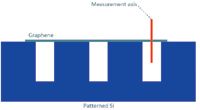
Figure 7: Graphene is suspended over holes in Si to determine the depth resolution. The red line displays the measuring position.
To probe this depth resolution one can perform a depth scan on silicon (Si), which shows a very small penetration depth for 532-nm excitation, is available in virtually every laboratory, and has a strong Raman signal. Following the discussion outlined for the lateral resolution, however, a very thin sample would be ideal. Graphene or ultrathin graphite (that is, 5–10 atomic layers) suspended over holes in Si is an ideal sample to illustrate this (see Figure 7 for a schematic of the sample). Similar to the CNTs for the lateral resolution, graphene has a very strong Raman signal and can act as an approximation for a delta function for the convolution of the sample geometry with the system function.
Figure 8a shows a depth profile of the integrated intensity of the first order Si peak (red) and the integrated intensity of the peak near 1600 rel. 1/cm recorded on suspended ultrathin graphite. The system used was an alpha300R microscope (WITec GmbH) with a 100× NA 0.9 Zeiss objective, a 10-µm pinhole (100 nm projected pinhole diameter), and a UHTS300 spectrometer (WITec GmbH). The integration time per point was 2 s and the step width was 50 nm. The z-position was set by an interferrometrically calibrated piezoelectric positioning table. The depth profiles in Figure 8a are offset for clarity. Figure 8b shows the spectrum of the ultrathin graphite in focus with a 2-s integration time.
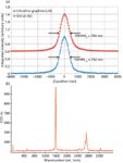
Figure 8: (a) Depth profile on suspended ultrathin graphite and Si. (b) A single spectrum on suspended ultrathin graphite (integration time 2 s).
A close comparison of the depth profile of Si with the one collected from ultrathin graphite shows that the rising part of the curve (negative z-position values; above the sample surface) are virtually identical. The falling half (positive z-position values; below the sample surface) shows a broadening for the Si curve. This broadening is because of the penetration of the laser into Si. This penetration depth is small for a green laser and Si, but would be considerably more for a near-IR laser and, thus, the curve of Si would be further distorted on the falling half. For excitation using a green laser source this comparison shows, however, that the commonly available Si can be used as a very good probe to obtain information on the depth resolution of a system.
Comparing these results to the theory for low numerical apertures illustrates that it cannot be valid for high numerical apertures. Converting this theory to match the high numerical aperture case is not trivial, but an approximation can be given following the work by Mack (14). Based on this, the ratio between the low numerical aperture and the high numerical aperture results can be calculated as

where θ is half of the opening angle of the objective. For an NA value of 0.9 this results in a correction factor of 1.38. Thus, the best depth resolution achievable according to this approximation should be about 682 nm.
The work by Wilhelm and colleagues (15) for confocal laser scanning microscopy can also be followed for this purpose. From this we find an axial optical resolution dependent on the projected pinhole size. For projected pinhole sizes larger than one "Airy unit" (1.22*λ/NA) the following equation applies:

where λem refers to the emitted wavelength. Using the experimental parameters shown above with λem = 580.7 nm, this results in an axial FWHM of 920 nm. It should be noted however, that the projected pinhole size is significantly smaller than the Airy unit in the presented data. For this case, the work by Wilhelm (15) suggests a different equation as follows:

With this, the calculated result is about 630 nm FWHM.
These theories do not result in the same axial resolution, which clearly indicates that there are some inconsistencies in the calculations (that is, between equations 4 and 6). It can however, clearly be seen both from the theories as well as experimentally, that FWHMs well below 1 µm are possible and can be expected from confocal Raman microscopes.
Summary
Confocal Raman microscopes allow the measurement of nanometer-size objects and, using such objects, the spatial resolution of the systems can be easily determined. The experimental results that are routinely achieved are very close to the theoretical predictions. The spectral resolution needs to be clearly defined and standard samples or light sources are best used to determine this. A reliable comparison should ideally duplicate all relevant parameters and, for example, require all resolution measurements to be performed using the same projected pinhole size.
Thomas Dieing, PhD, Marius Henrich, and Sonja Breuninger, PhD, are with WITec GmbH in Ulm, Germany. Direct correspondence to: sonja.breuninger@witec.de
References
(1) P. Jenniskens, M.H. Shaddad, D. Numan, S. Elsir, A.M. Kudoda, M.E. Zolensky, L. Le, G.A. Robinson, J.M. Friedrich, D. Rumble, A. Steele, S.R. Chesley, A. Fitzsimmons, S. Duddy, H.H. Hsieh, G. Ramsay, P.G. Brown, W.N. Edwards, E. Tagliaferri, M.B. Boslough, R.E. Spalding, R. Dantowitz, M. Kozubal, P. Pravec, J. Borovicka, Z. Charvat, J. Vaubaillon, J. Kuiper, J. Albers, J.L. Bishop, R.L. Mancinelli, S.A. Sandford, S.N. Milam, M. Nuevo, and S.P. Worden, Nature 458, 485–488 (2009).
(2) A. Rotundi, G.A. Baratta, J. Borg, J.R. Brucato, H. Busemann, L. Colangeli, L. D'Hendecourt, Z. Djouadi, G. Ferrini, I.A. Franchi, M. Fries, F. Grossemy, L.P. Keller, V. Mennella, K. Nakamura, L.R. Nittler, M.E. Palumbo, S.A. Sandford, A. Steele, and B. Wopenka, Meteorit. Planet. Sci. 43, 367–397 (2008).
(3) C. Heim, J. Lausmaa, P. Sjovall, J. Toporski, T. Dieing, K. Simon, B.T. Hansen, A. Kronz, G. Arp, J. Reitner, and V. Thiel, Geobiology 10, 280–297 (2012).
(4) S. Hild, F. Neues, N. Znidarsic, J. Strus, M. Epple, O. Marti, and A. Ziegler, J. Struct. Biol. 168, 426–436 (2009).
(5) N. Gierlinger and M. Schwanninger, Spectroscopy 21, 69–89 (2007).
(6) A. Hermelink, A. Brauer, P. Lasch, and D. Naumann, Analyst 134, 1149–1153 (2009).
(7) Y.N. Xu, D. Zhan, L. Liu, H. Suo, Z.H. Ni, T.T. Nguyen, C. Zhao, and Z.X. Shen, ACS nano 5, 147–152 (2011).
(8) Y. You, T. Yu, J. Kasim, H. Song, X. Fan, Z. Ni, L. Cao, H. Jiang, D. Shen, J. Kuo, and Z. Shen, Appl. Phys. Lett. 93, 103–111 (2008).
(9) T. Yu, Z. Ni, C. Du, Y. You, Y. Wang, and Z. Shen, J. Phys. Chem. C 112, 12602–12605 (2008).
(10) C. Matthaus, A. Kale, T. Chernenko, V. Torchilin, and M. Diem, Mol. Pharm. 5, 287–293 (2008).
(11) T. Chernenko, C. Matthaus, L. Milane, L. Quintero, M. Amiji, and M. Diem, ACS nano 3, 3552–3559 (2009).
(12) http://www.witec.de/en/download/Raman/StressinSi.pdf.
(13) T. Dieing, O. Hollricher, and J. Toporski, Confocal Raman Microscopy, (Springer, 2010) ISBN 978-3-642-12521-8.
(14) C.A. Mack, Microlithogr. World, February edition, 14–15 (2004).
(15) S. Wilhelm, B. Gröbler, M. Gluch, and H. Heinz, Confocal Laser ScanningMicroscopy, http://zeiss-campus.magnet.fsu.edu/referencelibrary/pdfs/ZeissConfocalPrinciples.pdf.

AI-Powered SERS Spectroscopy Breakthrough Boosts Safety of Medicinal Food Products
April 16th 2025A new deep learning-enhanced spectroscopic platform—SERSome—developed by researchers in China and Finland, identifies medicinal and edible homologs (MEHs) with 98% accuracy. This innovation could revolutionize safety and quality control in the growing MEH market.
New Raman Spectroscopy Method Enhances Real-Time Monitoring Across Fermentation Processes
April 15th 2025Researchers at Delft University of Technology have developed a novel method using single compound spectra to enhance the transferability and accuracy of Raman spectroscopy models for real-time fermentation monitoring.
Nanometer-Scale Studies Using Tip Enhanced Raman Spectroscopy
February 8th 2013Volker Deckert, the winner of the 2013 Charles Mann Award, is advancing the use of tip enhanced Raman spectroscopy (TERS) to push the lateral resolution of vibrational spectroscopy well below the Abbe limit, to achieve single-molecule sensitivity. Because the tip can be moved with sub-nanometer precision, structural information with unmatched spatial resolution can be achieved without the need of specific labels.