Advantages of High OD Filters to Microscopy
Application Notebook
The use of filters in optical microscopy has become so commonplace that it is hard to find a biological microscope that does not have some type of filter accessory kit. For particular modalities, such as two-photon imaging, the use of optical filters is essential to make the method viable. Filter technology has progressed steadily over the past few decades, moving away from simple colored glass filters to complicated thin-film–based optical components. With optical densities commonly reaching values of 4 or greater, spectrally selective imaging has never been more accurate.
Microscopists are all too familiar with the common issues of using colored glass for filtering out unwanted photons. Slow cut-on and cut-off transitions are problematic when using multiple fluorescent markers in a sample, making discrimination between individual markers almost impossible. Auto-fluorescence is also a confounding factor with filters of this type and can reduce the dynamic range of the instrument. Dielectric filters are the natural solution to these issues and have been a mainstay in the microscopy community for a long time.

Paul J. Gelsinger-Austin
The physical mechanism behind dielectric filters is based upon light's inherent ability to interfere with itself. This effect, eloquently described by Thomas Young to the Royal Society of England in 1801, manifests itself as periodic cancellations and enhancements of the light field across an observable area. Figure 1 illustrates the details of a simple interference experiment in which the combined intensity emitted by two very small apertures is observed at a screen very far away. For well-defined waves of light, the amplitudes of the electric field will add linearly at all positions in space. This makes the equation for the observed electric field Eobserved = E1 + E2. Because our eyes respond very slowly compared to the oscillation period of light waves, we observe the time-averaged energy that light carries with it, otherwise known as the "optical power" of the wave (typically measured in Watts). Therefore, the observed field that we would see in such an experiment is expressed as P = |Eobserved|2 = |E1 + E2|2. Presuming that the light waves are harmonic functions generally expressed in the form cos(Φ), we will expect to see periodic cancellations and enhancements of the light field at the observation plane. This was quite a revolutionary idea at the time, and helped pave the way for further developments of the electromagnetic wave theory of light. A more generalized and mathematical treatment of light fields was given by James C. Maxwell in 1873 in his Treatise on Electricity and Magnetism, which formed the foundation of the interaction of light with matter. From Maxwell's equations, we can derive the properties of thin films and hence, design customized wavelength-selective filters.
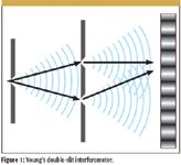
Figure 1
When one considers the physics of thin films, it is a slightly more complicated picture of Young's double-slit interferometer experiment. Instead of using point sources, we will consider the case of interfering plane waves of light, which can be thought of as the wavefronts generated by point sources that are very far away. As the distance from the point source increases, the wavefronts become more planar. In analyzing these plane waves, we will use the same assumption that Young used: Multiple beams of light that are derived from a common source can be combined using the superposition principle Eobserved = E1 + E2, and the observed energy flux per unit time is P = |Eobserved|2. The system we will consider is a thin film with index of refraction nfilm deposited onto a substrate with index of refraction ns. Such a system is illustrated in Figure 2. In this system, the interfering light sources are the reflections from the air-film interface (r1) and the film-substrate interface (r2), where the original wavefront is generated by a single point source located at infinity. Assuming a lossless medium and normal angle of incidence, the amplitude of the electric field reflected from each interface is given by the Fresnel amplitude coefficients:

In thin film design, the sign of the amplitude refection coefficient is very important. If we choose the optical path thickness of the film to be λ/4, the reflection coefficient r2 will change sign upon the light's return to the film–air interface from the substrate. Mathematically, this implies that at the surface of nfilm, the amplitude of the wavefront reflected from the film-substrate interface is –r2. In general, r1 will be negative because nfilm > 1. This means that if nfilm > ns, the interference of the two reflections will be additive (constructive). Conversely, if nfilm < ns, then the result will be subtractive (destructive). These two separate cases are what give rise to reflective and antireflective coatings. This is somewhat of an over-simplification of the physics, as it ignores multiple reflections, but it is a convenient device for understanding the nature of thin film interference.
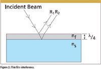
Figure 2
The choice of using a film thickness of λ/4 is a convention commonly used by coating designers specifically for the convention described earlier. A physically realized interference-based optical filter can consist of hundreds of layers λ/4 thick with alternating indices of refraction from low (L) to high (H), as shown in Figure 3. This type of configuration allows for the development of highly reflective and transmissive coatings with special wavelength properties. Typical families of filters generated using this basic design include high and low pass filters, bandpass filters, and notch filters. Unlike traditional colored glass filters, interference-based filters are highly customizable in terms of specifications such as cut-on and cut-off wavelengths (λc), bandwidth (Δλ), and out-of-band rejection (typically called the optical density, or OD). The optical density is an important parameter to consider when attempting to detect faint signals on a bright background, as is the case in fluorescence-based imaging. The optical density of a filter is defined by the logarithm of the ratio of transmitted to incident light.

Here, we have specifically noted that the optical density is related to wavelength. For many years, interference filters with an optical density of 4 (referred to as OD4) have been found commonly throughout the optics industry. It is a relatively new innovation to push beyond the OD4 barrier, where the main challenge has been to deposit more layers of material onto the filter substrate. A typical coating chamber is shown in Figure 4. Inside the chamber, a blank substrate is bombarded by vaporized material, which when cooled is the final coating. The coating process can be very long; it is not uncommon for a coating run to take as long as 3–5 h. For complicated coatings, much of this time is spent depositing the many alternating layers on the substrate, which can be anywhere from a handful to several dozen layers, depending upon the purpose of the filter. One of the biggest challenges for manufacturing coatings using the vapor deposition method is repeatability in the coating process between coating runs. Small variations in chamber pressure and temperature can cause significant irregularities in the formation and thickness of coating layers. Given that environmental changes in long coating runs can cause unpredictable coatings, a practical limit is placed upon the optical density of filters fabricated in this method. The use of colored glass as a substrate is sometimes required in order to achieve high optical densities with particular spectral filtering characteristics. This introduces absorption into the transmission band of the filter, resulting in bandpass filters with maximum transmission in the range 25–50%.
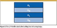
Figure 3
One of the big improvements to coating manufacturing has been the development of a technique known as magnetron sputtering. Unlike traditional vapor deposition techniques, magnetron sputtering does not require the coating material to be heated directly to apply it to the substrate. Instead, the process uses the ballistic properties of ionized argon to evaporate the coating material in a very controlled manner. Coating substrates in this way results in very dense coatings with few defects that have very high bonding energies with the substrate. Because the process is essentially "cold-evaporation," it allows the coating designer to use new materials, such as plastics and other low-melting-point insulators in the coating process, which opens up a new world of coating design. With this type of coating technique, the upper limit for the quantity of coating layers is over 200, resulting in filter designs with significantly higher optical densities in the realm of OD6. Current detector technologies limit the testing of filters to those with optical densities of OD6 or lower, although coatings theoretically can be designed to optical densities OD7 and greater. The ability to put down hundreds of layers on a substrate makes high opticaldensity filters a reality without the need for colored glass substrates, thereby permitting the manufacture of high optical density filters with very low autofluorescence.
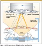
Figure 4
In addition to better out-of-band rejection, purely interference-based filters also exhibit better transmission properties than older OD4 filter designs, often improving bandpass filter transmission above 90%. The need for filters with this type of rejection is apparent in many areas of microscopy as well as light-starved, non-imaging techniques such as flow cytometry. For instance, switching from an OD4 to an OD6 filter in a fluorescence microscope can reduce the required operating power of the excitation source significantly and retain the same optical signal-to-background ratio. This is ideal for working with live biological samples, which may be "cooked" easily by the intense excitation energy in a fluorescence confocal or two-photon microscope. Even in traditional fluorescence microscopy, the increased in-band transmission provides a more vivid image of the selected fluorophore, as can be seen in Figure 5. In these images, the fluorescent microspheres are excited by an unfiltered broadband halogen light source. The two bandpass filters are centered about the yellow–red wavelength of 600 nm with bandwidths 80 nm (OD4) and 40 nm (OD6). The particular thing to notice between these two images is evident in the yellow fluorescent microspheres. Even though the OD4 filter has a larger bandwidth and hence, would allow more of the emission spectra to reach the detector, the OD6 image has brighter yellow microspheres. This is because the OD6 filter has an absolute transmission of ~90%, and the OD4 filter has an absolute transmission ~50%.
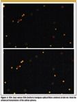
Figure 5
The advent of highly customizable interference filters creates an attractive option for researchers and OEMs alike. The improved transmission and higher optical density of filters manufactured using sputtering techniques makes them very suitable for many microscopy techniques, and in particular, those that target living tissue. Having complete control over spectral selection is essential to successfully determine the location and concentration of specific fluorescent molecules, and each increase in optical density is a step toward increased accuracy.
Paul J. Gelsinger-Austin earned his M.S. in Optical Sciences & Engineering from the University of Arizona (Optical Sciences Center). He is currently a Research & Development Engineer with Edmund Optics, Barrington, New Jersey.
References
(1) E. Hecht, Optics, 4th Ed. (Addison Wesley, San Francisco, 2002), pp. 426–430.
(2) J. Eastman, Optical thin film coatings. University of Rochester, Institute of Optics (1997).
(3) H. Macleod, Thin Film Optical Filters, 2nd Ed. (McGraw-Hill, New York, 1989).
(4) Introduction to Magnetron Sputtering. http://www.thermovacgen.com/catalogue/section-16/intro.htm, Accessed 02/12/09.
(5) Magnetron sputtering cathodes for magnetron sputtered thin films – What is sputtering? http://www.gencoa.com/1,120-What-is-sputtering.htm. Accessed 02/12/09.
(6) Sputtering technology. http://www.angstromsciences.com/technology/sputtering-technology/index.html. Accessed 02/12/09.
LIBS Illuminates the Hidden Health Risks of Indoor Welding and Soldering
April 23rd 2025A new dual-spectroscopy approach reveals real-time pollution threats in indoor workspaces. Chinese researchers have pioneered the use of laser-induced breakdown spectroscopy (LIBS) and aerosol mass spectrometry to uncover and monitor harmful heavy metal and dust emissions from soldering and welding in real-time. These complementary tools offer a fast, accurate means to evaluate air quality threats in industrial and indoor environments—where people spend most of their time.
NIR Spectroscopy Explored as Sustainable Approach to Detecting Bovine Mastitis
April 23rd 2025A new study published in Applied Food Research demonstrates that near-infrared spectroscopy (NIRS) can effectively detect subclinical bovine mastitis in milk, offering a fast, non-invasive method to guide targeted antibiotic treatment and support sustainable dairy practices.
Smarter Sensors, Cleaner Earth Using AI and IoT for Pollution Monitoring
April 22nd 2025A global research team has detailed how smart sensors, artificial intelligence (AI), machine learning, and Internet of Things (IoT) technologies are transforming the detection and management of environmental pollutants. Their comprehensive review highlights how spectroscopy and sensor networks are now key tools in real-time pollution tracking.