Automated Confocal Raman and Atomic Force Microscopy Imaging of Nanostructured Materials and Devices
Special Issues
The combination of confocal Raman and atomic force microscopes allows chemical and surface topography imaging of large samples without any ongoing process control by an operator. This article describes the relevant measurement principles and presents examples of automated measurements on nanostructured materials.
The development of nanostructured materials requires detailed knowledge of their chemical and structural properties, leading to a growing demand for characterization methods for heterogeneous materials on the nanometer scale. However, certain properties are difficult to study with conventional characterization techniques due to either limited resolution or the inability to differentiate materials chemically without inflicting damage or using invasive techniques such as staining. By combining various analytical techniques such as Raman spectroscopy, confocal microscopy, and atomic force microscopy (AFM) in one instrument, the same sample area can be analyzed nondestructively with these methods, providing a more complete understanding of the materials. Raman spectroscopy, a chemical analysis technique, combined with confocal microscopy, enables confocal Raman imaging (1–8). The power of Raman imaging stems from the extensive chemical information contained within molecular vibrational spectra. In the Raman spectral imaging mode, a complete Raman spectrum is recorded at every image pixel, producing a two-dimensional array consisting of tens of thousands of complete Raman spectra. From this array, images are extracted by analyzing various spectral features (such as sum, peak position, and peak width). Differences in chemical composition, although completely invisible in optical images, will be apparent in the Raman image and can be analyzed with a resolution down to 200 nm (3,6,9). The recently implemented high-speed electron multiplying charge coupled device (EMCCD) detector, in conjunction with an ultrahigh throughput spectrometer, allows a reduction in Raman data acquisition time by another factor of 20, down to 760 μs for a spectrum (ultrafast confocal Raman imaging) (10,11).
If higher resolution is required, the confocal Raman microscope can be transformed into an atomic force microscope by simply rotating the microscope turret. This technique is employed to trace the topography of samples with extremely high resolution by recording the interaction forces between the surface and a sharp tip mounted on a cantilever. The sample is scanned under the tip using a piezo-driven scan-stage, and the topography is reproduced with specialized software that translates this information into images. Structures below the diffraction limit can be visualized using this imaging technique (9). This article describes further improvements that allow the automated analysis of large samples with confocal Raman imaging and AFM. In addition to the acquisition of large area scans (12), it is possible to predefine measurement sequences at any user-defined selection of measurement points on the sample, guaranteeing the most comprehensive surface analysis tool for systematic and routine research tasks.
Instrumentation
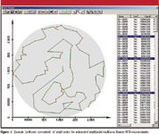
For the studies described here, a new microscopy system (WITec alpha500, Ulm, Germany) was used. It combines a high-throughput confocal Raman microscope for 3D chemical imaging and an atomic force microscope for high-resolution morphological imaging in an automated system for large samples. A piezo scanner, with a scan range of 200 μm × 200 μm, is mounted on top of a motorized xyz stage. This stage is driven by stepper motors and allows an extension of the scanning range along the x and y axes to 150 mm × 100 mm with a step size of 100 nm. As well as expanding the scanning range, this stage can be used to perform multiarea–multipoint measurements on any user-defined number of measurement points. An example of such a multipoint scan is shown in the software screenshot in Figure 1. The table on the right side lists the coordinates of the points of interest, whereas the graph on the left displays the points of interest and the travel path for automated point measurements. Through scripting functions, several consecutive tasks can be executed automatically without any online process control by an operator.

Figure 1
Example Measurements and Discussions
A series of AFM and Raman measurements were performed on a dynamic random access memory (DRAM) chip (Infineon Technologies, Neubiberg, Germany) to show the automation capabilities of the alpha500. In the first step, white light video images were recorded at three positions on the sample (Figure 2). The following scripts were used for this procedure: autoillumination for optimum white light illumination of the sample; autofocus to bring the sample into focus based upon the video images; and the snapshot acquires a video image at each preselected point.

Figure 2
The video images from Figure 2 were recorded with an Olympus 100× (NA = 0.95) objective and reveal the different patterns selected from the DRAM chip.
Parts of the three selected areas shown in Figure 2 were then imaged with Raman spectral imaging. In this imaging mode, a complete Raman spectrum is recorded at every image pixel, producing a 2D array of 150 × 150 Raman spectra. The integration time for each individual Raman spectrum was 10 ms; thus, the array of 22,500 Raman spectra was acquired in less than 4 min. By evaluating the position of the first order Si Raman band at 520/cm, stress images of the selected areas can be obtained (13). Figure 3 shows the stress images taken from the three preselected areas.

Figure 3
By simply rotating the microscope turret, the confocal Raman microscope was converted into an atomic force microscope. By using the same positions as used before for the acquisition of the Raman images, and the additional auto-tip-approach scripting function, AFM images were recorded from the same sample areas. Figure 4 shows the AFM images recorded from the three selected sample areas. The line structure in the area shown in the top image consists of parallel grooves that are 80 nm deep. The pits from areas shown in the other two images have a diameter of 300 nm and a depth of 300 nm.

Figure 4
Summary
By combining two nondestructive sample analysis methods in an automated system, precisely the same sample position can be investigated with either technique. Multipoint–multiarea measurements can be performed routinely at various areas on the sample. The motorized sample stage can be used to perform large overview scans, whereas the additional piezo-scan-stage allows the acquisition of high-resolution images from selected areas of the overview image. The implemented scripting routines, such as auto-focus and auto-AFM-tip-approach, guarantee standardized routine measurement procedures without any online process control by an operator during the measurement.
Ute Schmidt, Olaf Hollricher, Thomas Dieing, and Harald Fischer are with WITec GmbH, Ulm, Germany; www.witec.de
References
(1) O. Hollricher, OE Magazine, 17–20 (Nov. 2003).
(2) U. Schmidt, A. Jauss, W. Ibach, and O. Hollricher, Microscopy Today 13, 30 (2005).
(3) U. Schmidt, S. Hild, W. Ibach, and O. Hollricher, Macromol. Symp. 230, 133 (2005).
(4) A. Jauss and H. Fischer, Imaging and Microscopy 4, 24 (2005).
(5) U. Schmidt, Imaging and Microscopy 2, 34 (2005).
(6) A. Jauss, H. Fischer, and O. Hollricher, Imaging and Microscopy 1, 17 (2006).
(7) O. Hollricher, W. Ibach, A. Jauss, and U. Schmidt, FutureFab Intl 21, 136–138 (2006).
(8) U. Schmidt, W. Ibach, J. Mueller, and O. Hollricher, Proc. SPIE—Int. Soc. Opt. Eng. 6616 Pt. 1, 66160E-1 (2007).
(9) U. Schmidt, F. Vargas, T. Dieng, K. Weishaupt, and O. Hollricher, Nanotech. 4, 48 (2007).
(10) T. Dieing and O. Hollricher, Vib. Spectrosc., in press.
(11) Ultra-fast Confocal Raman Imaging, Application Note, www.witec.de 2008.
(12) alpha500 – Large area Scans of Tablets, WITec Application Note, www.witec.de 2008.
(13) U. Schmidt, W. Ibach, J. Mueller, K. Weishaupt, and O. Hollricher, Vib. Spectrosc. 42, 93 (2006).

AI-Powered SERS Spectroscopy Breakthrough Boosts Safety of Medicinal Food Products
April 16th 2025A new deep learning-enhanced spectroscopic platform—SERSome—developed by researchers in China and Finland, identifies medicinal and edible homologs (MEHs) with 98% accuracy. This innovation could revolutionize safety and quality control in the growing MEH market.
New Raman Spectroscopy Method Enhances Real-Time Monitoring Across Fermentation Processes
April 15th 2025Researchers at Delft University of Technology have developed a novel method using single compound spectra to enhance the transferability and accuracy of Raman spectroscopy models for real-time fermentation monitoring.
Nanometer-Scale Studies Using Tip Enhanced Raman Spectroscopy
February 8th 2013Volker Deckert, the winner of the 2013 Charles Mann Award, is advancing the use of tip enhanced Raman spectroscopy (TERS) to push the lateral resolution of vibrational spectroscopy well below the Abbe limit, to achieve single-molecule sensitivity. Because the tip can be moved with sub-nanometer precision, structural information with unmatched spatial resolution can be achieved without the need of specific labels.