Investigating Carbon Nanotubes Using Confocal Raman Microscopy and AFM
Carbon nanotubes are unique nanostructures with remarkable mechanical and electrical properties. Due to their tremendous potential for future innovations, great efforts are made to characterize these structures. In the following study, carbon nanotubes were investigated with Confocal Raman Microscopy and Atomic Force Microscopy using only one single instrument.

A thorough knowledge of structural and chemical properties is essential for the fields of nanotechnology and materials science, leading to a growing demand for characterization methods for heterogeneous systems on the nanometer scale. However, certain properties are difficult to study with conventional characterization techniques due to either limited resolution or the inability to chemically differentiate materials without inflicting damage or using invasive techniques such as staining. Confocal Raman microscopy can effectively overcome these fundamental obstacles.
A carbon nanotube is a member of the fullerene structural family forming cylindrical carbon molecules. Their name is derived from their size, because the diameter of a nanotube is on the order of a few nanometers, while they can be as much as several centimeters in length. Their remarkable mechanical and electrical properties make them potentially useful in a wide variety of applications (for example, nano-electronics, optics, materials applications). They exhibit extraordinary strength and unique electrical properties, and are efficient conductors of heat.
There are two main types of nanotubes: single-walled nanotubes and multiwalled nanotubes. Basically, the carbon nanotube is formed almost entirely, except for impurities, from simple carbon atoms (C). The structure of the carbon is a hexagonal lattice ("graphene sheet") rolled into a cylindrical tube, sometimes with a "cap" at each end of the cylinder (single-walled nanotube). Cylinders can exist inside other cylinders like the layers of a leek, with a gap of 0.34 nm between cylinders (multiwalled nanotube). Some pentagonal (five-sided) and heptagonal (seven-sided) defects can cause cylinders to bend, change diameter, or twist.
Well-established characterization methods for carbon nanotubes are scanning tunneling microscopy or transmission electron microscopy, allowing to measure the nanotube diameter or the chiral angle. However, the nanotubes can be damaged by the electron beam in the microscope. To nondestructively characterize the tubes, atomic force microscopy (AFM) and confocal Raman microscopy can be used. AFM reveals information on the structural morphology, whereas the Raman spectra of the tubes directly reflect the chemical composition and the molecular structure. For example, it is possible to identify the diameter of the tubes, their orientation depending upon polarization, different electrical properties, or even to distinguish single- and multiwalled nanotubes.
To show the capabilities of AFM and confocal Raman microscopy, in this study carbon nanotubes are investigated with a combined AFM/confocal Raman instrument. It is used to detect single nanotubes on a silicon substrate with the AFM mode. In a second step, Raman spectral imaging is performed to characterize the nanotubes more thoroughly.
Experimental
For the Raman and AFM measurements, a WITec Confocal Raman Microscope (alpha300) was used (WITec, Ulm, Germany). In Raman spectroscopy, a vibrational quantum stage is excited within a molecule, leading to an energy shift between the incident and the back-scattered light. This energy shift is unique to each molecule and allows the chemical identification of compounds within a sample. By integrating a sensitive Raman spectrometer within a state-of-the-art microscope setup, Raman microscopy with a spatial resolution down to 200 nm laterally and 500 nm vertically can be achieved using visible light excitation. Using the confocal arrangement, in which a pinhole is placed in the focal plane of the microscope to reject out-of-focus light, even depth profiling and 3-D imaging are possible if the sample is transparent. With this technique it is not only possible to obtain Raman spectra from extremely small sample volumes (down to 0.02 μm3 ), but also to collect high-resolution Raman images. Therefore, the CCD camera of the spectrometer is used to acquire a complete Raman spectrum at a user-defined number of image points per line, while the sample is scanned line by line. The number of image points (spectra) is limited only by the memory of the computer. A typical image consists of 10.000 (100 × 100) to 65.536 (256 × 256) spectra. From this multispectrum file, an image is computed by, for example, integrating over a certain Raman line in all spectra. The intensity calculated from each spectrum is color-coded and determines the brightness of the appropriate pixel in the image. As all spectra are stored in memory, a large variety of properties such as peak-width, center of mass, or peak position of certain Raman lines can be calculated from a single measurement and displayed as images. To collect a Raman image in a reasonable amount of time, special care must be taken to optimize the optical throughput and sensitivity of the setup. As a Raman image consists of several thousand pixels (spectra), the integration time per pixel (spectrum) must be as short as possible; because sample heating must be avoided, it is not possible to simply increase the laser power. In an optimized setup, the acquisition time per spectrum is typically less than 100 ms for most samples, so that Raman images of 100 × 100 pixels are obtained in little more than 15 min. A Nikon 100x (N.A.= 0.9) air objective was employed for all Raman measurements. For excitation, a NdYag laser (wavelength of 532 nm) was used.
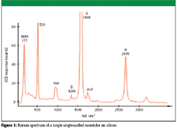
Figure 1
To perform AFM measurements, the same instrument, equipped with a special AFM objective, was used. It allows to switch between the Raman and the AFM mode by simply rotating the microscope turret without dislocation of the sample area. The AFM measurements were taken in AC Mode with Arrow FM cantilevers (Nanoworld, Germany) with a resonance frequency in the range of 70–90 kHz.
In the present experiment, laser vaporization-grown single-wall carbon nanotubes produced at Oak Ridge National Laboratory were imaged with the combined Raman/AFM System. The single-walled nanotubes were deposited on a silicon substrate using a spin-coating technique.
Results
Single-walled nanotubes exhibit three characteristic bands: the tangential (vibrations along the tube axis) stretching G mode (1500–1600 cm- ), which represents crystalline carbon, the D mode (1350 cm- ), and the radial breathing mode (100–400 cm- ), which frequency is inversely proportional to the tube diameter.
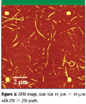
Figure 2
A detailed evaluation of the obtained spectral data of one carbon nanotube is shown in Figure 1. Each part of the spectrum, the radial breathing mode at around 180 cm- , the D-band at around 1340 cm- , the G-band at around 1590 cm- , second-order-modes, and the G-band can be used to differentiate properties of carbon nanotubes. The silicon lines at 520 cm- and at 960 cm- from the substrate are also visible.
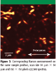
Figure 3
Figure 2 shows the AFM image of the nanotubes with a scan size of 14 μm × 14 μm and 256 × 256 pixels. Figure 3 shows the corresponding Raman measurement in the spectral imaging mode on the same sample position. Scan range is also 14 μm × 14 μm with 150 × 150 pixels (= 22,500 spectra) and an integration time of 50 ms per spectrum. The image was obtained by integrating over the prominent Raman line of carbon nanotube at 1588 cm- . Visible are only nanotubes which are parallel to the polarization axis.
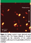
Figure 4
By comparing the Raman image with the AFM topography, it is clear that single carbon nanotubes are observed in the Raman spectral imaging mode.
To show the influence of the polarization axis of the excitation light, a second experiment was carried out. Therefore, two measurements with different polarization orientation were performed on the same sample area. As can be seen from the images, the Raman signal is always strongest when the laser light is polarized along the nanotube axis (compare Figures 4 and 5).
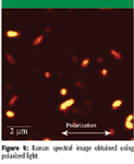
Figure 5
Conclusion
Due to its modular design, a combined confocal Raman/AFM microscopy system is a universal and scalable tool for a variety of applications. By combining AFM and Raman data, single carbon nanotubes can be localized in AFM topography images and their structure can then be analyzed by confocal Raman microscopy. The ability to then acquire Raman images of single nanotubes provides scientists nouvelle opportunities to study the chemical composition of the nanotubes, to identify the direction of the polarization in the tubes, to distinguish carbon nanotubes from other carbon materials or polymers, to sort the nanotubes by length or diameter, and even to distinguish between single- and multiwalled nanotubes.
Andrea Jauss, Harald Fischer, and Olaf Hollricher are with WITec, Ulm, Germany.

AI-Powered SERS Spectroscopy Breakthrough Boosts Safety of Medicinal Food Products
April 16th 2025A new deep learning-enhanced spectroscopic platform—SERSome—developed by researchers in China and Finland, identifies medicinal and edible homologs (MEHs) with 98% accuracy. This innovation could revolutionize safety and quality control in the growing MEH market.
New Raman Spectroscopy Method Enhances Real-Time Monitoring Across Fermentation Processes
April 15th 2025Researchers at Delft University of Technology have developed a novel method using single compound spectra to enhance the transferability and accuracy of Raman spectroscopy models for real-time fermentation monitoring.
Nanometer-Scale Studies Using Tip Enhanced Raman Spectroscopy
February 8th 2013Volker Deckert, the winner of the 2013 Charles Mann Award, is advancing the use of tip enhanced Raman spectroscopy (TERS) to push the lateral resolution of vibrational spectroscopy well below the Abbe limit, to achieve single-molecule sensitivity. Because the tip can be moved with sub-nanometer precision, structural information with unmatched spatial resolution can be achieved without the need of specific labels.