Article
Spectroscopy
Spectroscopy
Next-Generation Mid-Infrared Chemical and Biological Sensors: Combining Quantum Cascade Lasers with Thin-Film and Hollow Waveguides
Author(s):
Mid-infrared (MIR, 3-20 µm) sensor platforms are increasingly adopted in chem/bio analytics, and applied in areas ranging from process monitoring to medical diagnostics. Due to the inherent access to molecule-specific fingerprints via well-pronounced fundamental vibrational, rotational, and roto-vibrational transitions, quantitative information at ppm to ppb concentration levels and beyond is achievable in solids, liquids, and gases. In particular, the combination of quantum cascade lasers (QCLs) with correspondingly tailored waveguide technologies serving as optical transducers – thin-film waveguides for liquid/solid phase analysis, and substrate-integrated hollow waveguides for gaseous samples – facilitates miniaturizable and integrated optical chem/bio sensors and diagnostics applicable in, e.g., exhaled breath analysis, food safety, and environmental monitoring.
Mid-infrared (MIR, 3–20 μm) sensor platforms are increasingly adopted in chemical and biological analysis, and they are applied in areas ranging from process monitoring to medical diagnostics. Because of the inherent access to molecule-specific fingerprints via well-pronounced fundamental vibrational, rotational, and rotovibrational transitions, quantitative information at parts-per-million to parts-per-billion concentration levels and beyond is achievable in solids, liquids, and gases. In particular, the combination of quantum cascade lasers (QCLs) with correspondingly tailored waveguide technologies serving as optical transducers-thin-film waveguides for liquid–solid phase analysis, and substrate-integrated hollow waveguides for gaseous samples-facilitates the use of miniaturizable and integrated optical chemical and biological sensors and diagnostics for applications such as exhaled breath analysis, food safety, and environmental monitoring.
Recent developments in materials science and semiconductor technologies, particularly during the past two decades, have led to diagnostic tools based on mid-infrared (MIR: 2–20 µm, 400–4000 cm-1) sensing principles. Although infrared (IR) spectroscopy is routinely used in laboratories for applications such as qualitative process analysis, synthesis control, and bioanalytics, IR techniques applied for in-field or point-of-care (POC) scenarios remain rather limited. Besides the inherent qualitative information provided by molecular fingerprint absorptions, quantitative information may be derived following the Beer-Lambert law-that is, A = cdε, which relates the determined absorbance (A) at a specific wavelength or within a wavelength window to the analyte concentration (c) at a given sample thickness or optical pathlength (d) via the molar absorption coefficient ε. In addition to appropriate instrument dimensions, on-site usage of IR instrumentation frequently requires the availability of infrastructure such as purging gases. A size reduction of conventional IR spectroscopic instrumentation-for example, for a Fourier transform infrared (FT-IR) spectrometer-requires scaling of the optical building blocks, including the black body light source and interferometer, which is usually accompanied by reduced performance (1).
Consequently, advanced light sources such as tunable quantum cascade or interband cascade lasers, arrays thereof, or frequency combs based on this technology, combined with appropriately designed waveguides or transducers and integrated detection schemes, facilitate compact spectroscopic and sensing devices in the MIR spectral window without compromising performance compared to full-size systems.
Light Sources in the Mid-Infrared
Tunable quantum cascade lasers (tQCLs) (2) and interband cascade lasers (ICLs) (3) are promising alternatives to conventional (for example, thermal) black body radiators. When using tunable laser light sources, wavelength selection is inherent to the radiation source and does not require additional optical components. QCLs were first theoretically described in 1971 by Kazarinov and colleagues (4), and reduced to practice in 1994 by Faist and colleagues (5). Epitaxially grown semiconductor structures provide periodically repeated stacks of quantum well heterostructures (for example, semiconductor superlattices) allowing for discrete intersubband transition of electrons injected within the conduction band of such devices (Figure 1a). The injected electrons are sequentially transiting via appropriately cascaded potential barriers, ideally emitting a photon upon relaxation into a lower energy quantum well. Multiplication of these quantum heterostructures leads to a cascade effect with each electron responsible for the emission of multiple photons, thereby achieving higher quantum efficiencies than conventional laser diodes. QCLs may be realized via Fabry-Pérot structures or using Bragg reflectors, providing for single-mode emission in a distributed feedback (DFB) architecture. Tuning of the emission wavelength of such monolithically structured devices may be realized-in narrow wavelength ranges of about 0.2 % of the central wavelength (6)-via temperature or applied current. Broader tuning ranges are realized via an external cavity (EC) QCL configuration defining the amplified wavelength in the resonator structure via external diffraction gratings, albeit at the cost of additional mechanical tuning optics. Using EC structures, however, tuning ranges of up to 400 cm-1 at tuning rates of up to 1000 cm-1s-1 may be realized at individual QCL chips.
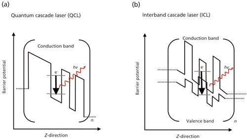
Figure 1: Simplified scheme of the band structure in (a) a quantum cascade laser (QCL) and (b) an interband cascade laser for n periodically stacked layers of quantum hetero structures of semiconductor materials that create subbands in the conduction band (QCL) and the valence band (ICL) of the laser structure. In QCLs, injected electrons (dashed lines symbolize injection regions) emit radiation when relaxing via intersubband transitions into lower energy quantum wells. In ICLs, injected electrons emit radiation via transitions from the conduction band into the valence band. The band structure in (b) is tailored such that the conduction band of one material layer is at lower energy vs. the valence band of the adjacent material, which facilitates the reinjection of electrons.
Interband cascade lasers (ICLs) fabricated of antimony or arsenide alloy based materials operating in the MIR provide an optical power output of several tens of milliwatts, but with lower electrical power consumption compared to QCLs (3). ICLs were theoretically described in 1995 by Yang and colleagues (7), and room-temperature continuous wave (CW) operation was demonstrated in 2008 (8). In lieu of subband transitions, radiation is generated via interband transitions between the conduction band and the valence band (Figure 1b). The so-called type II design entails that the conduction band minimum of one band is lower than the valence band maximum, which enables an increased effectivity of reinjecting electrons. With this design, ICLs provide a power-efficient alternative to QCLs for applications where low-power operation in CW mode at ambient temperatures is essential, whereas QCLs generally provide higher optical power output, wider tuning ranges, and emission well into the molecular fingerprint regime that is, > 10 µm).
Advanced Optical Transducers for Mid-Infrared Chemical and Biological Sensing
Thin-Film Waveguides
Whereas transmission experiments are especially suitable for optically rare samples, such as gaseous analytes, evanescent field absorption techniques with a distinct penetration depth dp of the radiation propagating within in appropriated waveguide (9,10) are useful for probing opaque, strongly absorbing, predominantly liquid or solid samples. Liquid water, which is ubiquitous in biological or biomedical analyte matrices, is a particularly strong infrared absorber, and frequently limits the penetrable sample thickness (d) in transmission absorption spectroscopy. IR-transparent waveguide materials include bulk crystals made from silicon (Si), germanium (Ge), or zinc selenide (ZnSe), and they are widely used as macroscopic internal reflection elements (IREs) in infrared attenuated total reflection (IR-ATR) spectroscopy. However, single-mode wave propagation is achieved only by reduction of macroscopic waveguiding crystals to a microscale, and one or several individual internal reflections are effectively replaced by a homogeneous evanescent field at the waveguide–sample interface. Tailoring the material composition and dimensions of waveguides to suit the demands of infrared sensing in combination with laser light sources such as QCLs and ICLs enables users to probe minute sample volumes, quantities, and concentrations at a yet unprecedented level of device integration (11,12).
Because of recent advances in materials science and microfabrication (13), thin-film waveguide structures transparent throughout the MIR spectral band based on materials such as diamond, mercury–cadmium–telluride (MCT), silver halides (AgCl; AgBr; AgBr1-x/Clx), germanium (Ge), and gallium arsenide (GaAs) have become readily available. Frequency-tailored thin-film waveguides ideally match the unique properties of QCLs and ICLs and serve as highly efficient optical transducers in infrared chemical and biological sensing scenarios. For example, the physical hardness, chemical inertness, and biocompatibility of diamond make it especially suitable for various sensing tasks, including probing protein conformation changes in solutions and investigating concentration changes of molecular analytes within aggressive media (14–17). Thin-film silver halide structures may be deposited at comparatively lower cost on silicon substrates, facilitating the combination of IR transducers with complementary metal-oxide-semiconductor (CMOS) devices (18) and integrated circuits for chip-level integration of chemical–biological sensing architectures within complementary control electronics and circuitry. Germanium-based thin-film waveguides have been demonstrated for the detection of cocaine within a microfluidic device (19). Albeit being relatively exotic, MCT-based waveguide structures may allow for the monolithic integration of waveguide and detector structures within a single device (20,21). Last but not least, III-V semiconductors including GaAs/AlGaAs systems have nowadays evolved into the probably most mature on-chip thin-film MIR waveguide technology because of their wide transparent window (approximately 0.9–15 µm) in the MIR. The refractive indices of GaAs and aluminum gallium arsenide (AlxGa1-x As) may be tailored straightforwardly via varying the aluminum content in the AlGaAs structures. Thus, the refractive index contrast between the optical buffer layer and the actual waveguide deposited on top results in monolithic transducer devices tailored toward highly efficient mode conservation and waveguiding properties. Usually, molecular beam epitaxy (MBE) and metal organic vapor phase epitaxy (MOVPE) are applied for growing accordingly designed structures at a wafer scale (13,22). Further waveguide structuring is then executed using conventional photolithographic patterning along with wet and dry etching protocols. As a result, a wide variety of waveguide designs have been realized (23), including ridge, rib, and strip waveguides, Mach-Zehnder interferometer (MZI) structures (24,25), ring resonators, and surface plasmon resonance (SPR) grating structures, as shown exemplarily in Figure 2 (26).
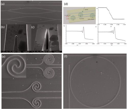
Figure 2: Advanced transducer structures fabricated from GaAs/AlGaAs thin-film waveguides. (a) Mach-Zehnder interferometer (MZI) structures with reshaped Y-couplers (b,c) via focused ion beam (FIB) milling. (d) Analytical signal of the device shown in (a). (e) Spiral arms within a MZI structure for enhancing the effective interaction path length. (f) Ring resonator structure tailored for mid-infrared wavelengths. Partially reprinted with permission from the American Chemical Society.
For chemical and biological sensing applications it should be noted that GaAs surface chemistry is closely related to that of gold, thus allowing for the application of well-established thiol chemistry (such as self-assembled monolayers and SAMs) as immobilization architecture. Thereby, stable surface modifications such as device passivation, analyte recognition and capture, and signal enhancement via plasmonic nanoparticles are enabled (24,27).
Mizaikoff and colleagues (28,29) have recently shown appropriate macroscopic packaging for developing GaAs/AlGaAs technologies into applicable structures suitable for IR-lab-on-chip systems. The utility of QCL-based sensors combined with on-chip waveguide technologies (Figure 3) has been demonstrated for the dynamic detection of environmentally relevant chlorinated hydrocarbons in aqueous media in a chemical sensing configuration (30). In another example relevant in food and feed contamination analysis, solid samples and liquid extracts have been studied for the determination of fungal infection and mycotoxin contamination levels in matrices such as maize, wheat, and peanuts (31,32).
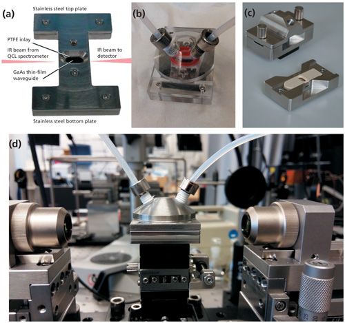
Figure 3: Infrared sensor platform utilizing thin-film waveguides within a macroscopic package: (a) Stainless steel base plate with direct access to the GaAs/AlGaAs thin-film waveguide for the analysis of solid samples, (b, c) assembled flow cell for continuous analysis of liquids in a flow-through sensing scenario (transparent PMMA device for demonstration purposes only), (d) stainless steel flow-cell assembly for readily combining thin-film waveguide structures with QCL or ICL base spectroscopy and sensing scenarios. Copyright by MIRa-Guide, MG Optical Solutions, Utting, Germany. Partially reprinted with permission from American Chemical Society.
Despite the utility of these device concepts, it remains essential to apply advanced multivariate calibration and classification algorithms including, for example, principal components analysis and regression (PCA and PCR), partial least squares regression (PLS), and artificial neural network (ANN) algorithms for maximizing the reliability of qualitative and quantitative information extracted from the spectral data resulting from complex analyte matrices (33).
Substrate-Integrated Hollow Waveguides
In contrast to solid-state waveguides guiding light via internal reflection, hollow waveguides (HWGs) propagate IR radiation within a hollow core structure coated on the inside with an IR reflective material such as silver, gold, or aluminum. Hence, such structures may simultaneously serve as a light guide (also known as a “light pipe”) and as a miniature gas cell. Mizaikoff and colleagues have innovatively expanded this concept via so-called substrate-integrated hollow waveguide structures (iHWGs), which ideally lend themselves for gas- and vapor-phase sensing applications requiring minute sample volumes and rapid sample transition times. To date, iHWGs have been applied predominantly in the near infrared (NIR) for the simultaneous quantitative analysis of mixtures of n-alkanes (for example, methane, ethane, propane, and butane) (48), and in the MIR for the detection of H2S and SO2 (49).
Although the combination of compact FT-IR spectrometers with iHWGs provides for a broad accessible spectral window, again the combination with QCLs (and more recently ICLs) facilitates enhanced signal-to-noise ratios (S/N)-and therefore lower limits of detection in tunable diode laser absorption spectroscopy (TDLAS) configurations-along with substantial device miniaturization (34–38). Early sensor designs based in part on photonic band gap hollow waveguides (39) were used for the detection of volatile organic compounds (VOCs) including CO, CO2, CH4, C2H4, xylenes, and NOX species (39–44), with the latter of particular interest in catalysis research (45). These early designs required elongated hollow fibers for obtaining suitable optical pathlengths facilitating trace gas detection. Alternatively, iHWGs (46) provide extremely robust transducer devices fabricated from materials such as thermoplastics, brass, and aluminum, in part with subsequent surface coating-for example, via electroplated gold. In addition, iHWGs enable the integration of meandered hollow waveguide structures, thereby providing extended optical pathlengths and maintaining overall compact device dimensions. Last but not least, they are easy to fabricate using conventional milling (metal substrate) or extrusion (plastic substrate) strategies, and may readily be tailored to specific application scenarios (47). Using similar device footprints, the integration of additional functionalities such as a photoconversion module or a preconcentration structure have been demonstrated for the detection of compounds such as ozone or hydrogen sulfide (50,51) at low parts-per-million-by-volume concentration levels (Figure 4).
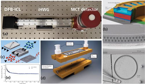
Figure 4: Gas sensing systems based on substrate-integrated hollow waveguide (iHWG) structures: (a) Distributed feedback interband cascade laser (DFB-ICL) coupled to an iHWG and an MCT detector, (b) schematic layout and scanning electron microscopy (SEM) images of a dual-color quantum cascade ring resonator laser that readily couples to an iHWG device, (c) schematic of an integrated device comprising a preconcentrator, a photoconverter, and an iHWG architecture for advanced gas sensing scenarios, (d, e) straight iHWG and performance test for CO detection in comparison with gas chromatographic studies. a, c, reprinted with permission from the American Chemical Society. b, d, and e reprinted with permission from The Royal Society of Chemistry.
Most recently, the utility of such devices for trace analyte detection in exhaled breath diagnostics has been demonstrated (53). For example, isoprene in exhaled breath has been detected at a limit of quantification of approximately 100 ppb (54), which demonstrates the potential of this approach for point-of-care (POC) diagnostics, continuous monitoring in respirator-ventilator scenarios in intensive care units (ICUs), and-assuming further device integration and cost reduction-for personalized health care applications.
Conclusions
The combination of MIR laser light sources such as QCLs and ICLs with advanced optical transducers, waveguides, and sampling interfaces is a versatile alternative to conventional IR spectrometers for a variety of different analytical application scenarios, analytes, and sample matrices. Advances in both laser light source technology and design of transducer structures has enabled significant improvement in device performance, while at the same time significantly reducing the overall device footprint. Furthermore, the inherent molecular specificity in the mid-infrared spectral regime along with minimal sample preparation-or likewise integrated sample conversion and preconcentration strategies-allow for trace analysis in liquids, solids, and gases. Further miniaturization and integration of the radiation source, optical transducer, and detector clearly pave the way toward true IR-lab-on-chip concepts. It is anticipated that such devices are not only applicable in point-of-care diagnostics in medical and clinical environments, but in any application scenario that requires possibly compact, mobile, and portable sensing units giving access to quantitative molecular fingerprints.
References
- J. Haas and B. Mizaikoff, Annu. Rev. Anal. Chem., 1–24 (2016).
- L. Zhang, G. Tian, J. Li and B. Yu, Appl. Spectrosc.68, 1095–1107 (2014).
- I. Vurgaftman, R. Weih, M. Kamp, J. R. Meyer, C.L. Canedy, C.S. Kim, M. Kim, W.W. Bewley, C.D. Merritt, J. Abell, and S. Höfling, J. Phys. D. Appl. Phys.48, 123001 (2015).
- R.F. Kazarinov and R.A. Suris, Sov. Phys. - Semicond.5, 707–709 (1971).
- J. Faist, F. Capasso, D.L. Sivco, C. Sirtori, A.L. Hutchinson, and A.Y. Cho, Science264, 553–556 (1994).
- Y. Bidaux, A. Bismuto, C. Tardy, R. Terazzi, T. Gresch, S. Blaser, A. Muller, and J. Faist, Appl. Phys. Lett.107, 221108 (2015).
- R.Q. Yang, Superlattices Microstruct.17, 77–83 (1995).
- M. Kim, C.L. Canedy, W.W. Bewley, C.S. Kim, J.R. Lindle, J. Abell, I. Vurgaftman, and J.R. Meyer, Appl. Phys. Lett.92, 191110 (2008).
- N.J. Harrick, Internal Reflection Spectroscopy (John Wiley & Sons Inc., New York, 1967).
- J. Fahrenfort, Spectrochim. Acta 17, 698–709 (1961).
- B. Mizaikoff, Chem. Soc. Rev.42, 8683–8699 (2013).
- M. Sieger and B. Mizaikoff, Anal. Chem.88, 5562–5573 (2016).
- B. Mizaikoff, X. Wang, M. Sieger, L. Faraone, J. Antoszewski, W. Lei, M. Jetter, and P. Michler, 2014 Conf. Optoelectron. Microelectron. Mater. Devices, COMMAD 2014, 301–302 (2014).
- X. Wang, M. Karlsson, P. Forsberg, M. Sieger, F. Nikolajeff, L. Österlind, and B. Mizaikoff, Anal. Chem. 86, 8136–8141 (2014).
- Á.I. López-Lorente and B. Mizaikoff, Anal. Bioanal. Chem., 408. 2875–2889 (2016).
- Á.I. López-Lorente, P. Wang, M. Sieger, E. Vargas Catalan, M. Karlsson, F. Nikolajeff, L. Österlund, and B. Mizaikoff, Phys. status solidi213, 2117–2123 (2016).
- M. Janotta, F. Vogt, H. Voraberger, W. Waldhauser, J. M. Lackner, C. Stotter, M. Beutl, and B. Mizaikoff, Anal Chem. 76, 384–391 (2004).
- T. Lewi and A. Katzir, Opt. Lett.37, 2733 (2012).
- Y.-C. Chang, P. Wägli, V. Paeder, A. Homsy, L. Hvozdara, P. van der Wal, J. Di Francesco, N.F. de Rooij, and H. Peter Herzig, Lab Chip12, 3020 (2012).
- X. Wang, J. Antoszewski, G. Putrino, W. Lei, L. Faraone, and B. Mizaikoff, Anal. Chem.85, 10648–10652 (2013).
- W. Lei, J. Antoszewski and L. Faraone, Appl. Phys. Rev.2, 41303–33 (2015).
- C. Charlton, M. Giovannini, J. Faist, and B. Mizaikoff, Anal. Chem.78, 4224–4227 (2006).
- M. Sieger and B. Mizaikoff, Photon. Res.4, 106–110 (2016).
- L. Leidner, M. Ewald, M. Sieger, and B. Mizaikoff, Proc. SPIE8774, 1–15 (2013).
- M. Sieger, F. Balluff, X. Wang, S. Kim, L. Leidner, G. Gauglitz, and B. Mizaikoff, Anal. Chem.85, 3050–3052 (2013).
- Ó. Esteban, A. González-Cano, B. Mizaikoff, N. Díaz-Herrera, and M.C. Navarrete, Plasmonics7, 647–652 (2012).
- C. Kirchner, M. George, B. Stein, W. Parak, H. Gaub, and M. Seitz, Bayreuth Polym. Symp. Int. Symp. Funct. Struct. Polym. Mater., 12, 266–276 (2001).
- M. Sieger, J. Haas, M. Jetter, P. Michler, A. Katzir, M. Godejohann, and B. Mizaikoff, Anal. Chem. 88, 2558–2562 (2016)
- MIRa-Guide, MG Optical Solutions, Utting, Germany.
- J. Haas, R. Stach, M. Sieger, Z. Gashi, M. Godejohann, and B. Mizaikoff, Anal. Methods, 8. 6602–6606 (2016).
- D. McMullin, B. Mizaikoff, and R. Krska, Anal. Bioanal. Chem.407, 653–660 (2014).
- M. Sieger, G. Kos, M. Sulyok, M. Godejohann, and R. Krska, Sci. Rep., submitted (2016).
- G. Kos, M. Sieger, D. McMullin, C. Zahradnik, M. Sulyok, T. Öner, B. Mizaikoff, and R. Krska, Food Addit. Contam. Part A33, 1596–1607 (2016).
- L. Hvozdara, S. Gianordoli, G. Strasser, W. Schrenk, K. Unterrainer, E. Gornik, M. Kraft, V. Pustogow, and B. Mizaikoff, Phys. E7, 37–39 (2000).
- L. Hvozdara, S. Gianordoli, G. Strasser, W. Schrenk, K. Unterrainer, E. Gornik, C.S.S.S. Murthy, M. Kraft, V. Pustogow, B. Mizaikoff, A. Inberg, and N. Croitoru, Appl. Opt.39, 6926 (2000).
- E. Tütüncü, V. Kokoric, R. Szedlak, D. MacFarland, T. Zederbauer, H. Detz, A. M. Andrews, W. Schrenk, G. Strasser, and B. Mizaikoff, Analyst,141, 6202–6207 (2016).
- E. Tütüncü, M. Nägele, P. Fuchs, M. Fischer, and B. Mizaikoff, ACS Sensors1, 847–851 (2016).
- C. Young, S.-S. S. Kim, Y. Luzinova, M. Weida, D. Arnone, E. Takeuchi, T. Day, and B. Mizaikoff, Sensors Actuators B Chem.140, 24–28 (2009).
- C. Charlton, B. Temelkuran, G. Dellemann, and B. Mizaikoff, Appl. Phys. Lett.86, 1–3 (2005).
- S.S. Kim, N. Menegazzo, C. Young, J. Chan, C. Carter, and B. Mizaikoff, Appl. Spectrosc.63, 331–337 (2009).
- O.A. Pogodina, V.V. Pustogov, F. De Melas, C. Haberhauer-Troyer, E. Rosenberg, H. Puxbaum, A. Inberg, N. Croitoru, and B. Mizaikoff, Anal. Chem.76, 464–468 (2004).
- C.R. Young, N. Menegazzo, A.E. Riley, C.H. Brons, F.P. Disanzo, J.L. Givens, J.L. Martin, M.M. Disko, and B. Mizaikoff, Anal. Chem.83, 6141–6147 (2011).
- B.T. Thompson, A. Inberg, N. Croitoru, and B. Mizaikoff, Appl. Spectrosc.60, 266–271 (2006).
- B. Mizaikoff, Photonics Spectra 40, 64–68 (2006).
- V. Kokoric, D. Widmann, M. Wittmann, R.J. Behm, and B. Mizaikoff, Analyst141, 5990–5995 (2016).
- A. Wilk, J.C. Carter, M. Chrisp, A.M. Manuel, P. Mirkarimi, J.B. Alameda, and B. Mizaikoff, Anal. Chem.85, 11205–11210 (2013).
- P.R. Fortes, J.F. da Silveira Petruci, A. Wilk, A.A. Cardoso, I.M. Raimundo Jr., and B. Mizaikoff, J. Opt.16, 94006 (2014).
- R.L. Ribessi, T. de A. Neves, J.J. R. Rohwedder, C. Pasquini, I.M. Raimundo, A. Wilk, V. Kokoric, and B. Mizaikoff, Analyst141, 5298–5303 (2016).
- J.F. da Silveira Petruci, P.R. Fortes, V. Kokoric, A. Wilk, I.M. Raimundo, A.A. Cardoso, and B. Mizaikoff, Analyst139, 198–203 (2014).
- J.F.D.S. Petruci, A.A. Cardoso, A. Wilk, V. Kokoric, and B. Mizaikoff, Anal. Chem., 87, 9580–9583 (2015).
- J.F. da Silveira Petruci, A. Wilk, A.A. Cardoso, and B. Mizaikoff, Anal. Chem.87, 9605–9611 (2015).
- F. De Melas, V. Pustogow, D.D.K. Wolcott, F. de Melas, D.C. Olson, A. Inberg, N. Croitoru, B. Mizaikoff, and V.V. Pustogov, Int. J. Environ. Anal. Chem. 83, 573–583 (2003).
- K. Wörle, F. Seichter, A. Wilk, C. Armacost, T. Day, M. Godejohann, U. Wachter, J. Vogt, P. Radermacher, and B. Mizaikoff, Anal. Chem.85, 2697–2702 (2013).
- D. Perez-Guaita, V. Kokoric, A. Wilk, S. Garrigues, and B. Mizaikoff, J. Breath Res.8, 26003 (2014).
- a Piotrowski, P. Madejczyk, W. Gawron, K. Klos, M. Romanis, M. Grudzien, J. Piotrowski, and A. Rogalski, Opto-Electronics Rev.12,453–458 (2004).
- A. Reyes-Reyes, R.C. Horsten, H.P. Urbach, and N. Bhattacharya, Anal. Chem.87, 507–512 (2015).
Julian Haas, Erhan Tütüncü, Andreas Wilk, Vjekoslav Kokoric, and Boris Mizaikoff are with the Institute of Analytical and Bioanalytcal Chemistry, Ulm University, Albert-Einstein-Allee 11, 89081 Ulm, Germany. Direct correspondence to: boris.mizaikoff@uni-ulm.de

Newsletter
Get essential updates on the latest spectroscopy technologies, regulatory standards, and best practices—subscribe today to Spectroscopy.


