Effect of Layer Number and Crystal Stacking Orientation on the Raman Spectra of Two-Dimensional MoS2
Spectroscopy
Raman imaging provides detailed crystal orientation information for two-dimensional MoS2 prepared by chemical vapor deposition on silicon substrates. These two-dimensional crystals consist of individual atomic layers of sulfur, molybdenum, and sulfur atoms.
The number of stoichiometric layers and crystal stacking orientation affect the Raman spectra of two-dimensional MoS2 prepared by chemical vapor deposition on silicon substrates. Raman imaging in the low-energy region of the spectrum is used to reveal the spatial variation of the single, double, and triple trilayers in MoS2. Crystals with different stacking orientation were analyzed by Raman spectroscopy. The low-energy shear and interlayer breathing modes peak positions and signal strengths depend on the parallel or anti-parallel crystal stacking orientation as the number of trilayers increase. The progression of relative peak positions in a crystal with parallel trilayer orientation is the opposite of that observed for crystals with anti-parallel trilayer orientation.
We have discussed Raman spectroscopy and imaging of few-layer exfoliated MoS2 low-energy phonons in a previous installment of “Molecular Spectroscopy Workbench” (1). These two-dimensional (2D) crystals are structures consisting of individual atomic layers of sulfur, molybdenum, and sulfur atoms corresponding to the stoichiometric unit of MoS2. The plane of molybdenum atoms is sandwiched above and below by planes of sulfur atoms. Therefore, we describe each stoichiometric layer in a crystal of MoS2 as a trilayer of sulfur, molybdenum, and sulfur atomic planes. In recent years, new inorganic 2D materials have emerged, including MoS2, MoSe2, WS2, and WSe2, among others. These materials have attracted significant interest because of special electronic, optical, and optoelectronic properties in the single trilayer to few-layer forms that are different from those manifest by the bulk form (2,3). One of the most important differences of the 2D crystals is the transformation from an indirect band gap semiconductor in the bulk, to a direct band gap semiconductor in the single trilayer, to few-layer crystals. Thus, the fabrication of optoelectronic devices in addition to familiar integrated electronic circuitry is envisioned for these materials. These optoelectronic characteristics have prompted substantial research to discover the means of fabrication and the physical characteristics of two-dimensional crystals to produce integrated electronic and optoelectronic devices (3).
There is a great need to characterize these materials and correlate the solid-state structure to their physical properties. The experimental nature of these materials leads to structural variability often within a single film. Consequently, there have been attempts to develop analytical methods for the reliable characterization of 2D crystals. You may have observed the spatially varying colors in reflected white light images of nanomaterials, and so there have been developments to use optical microscopy to rapidly identify the number of stoichiometric layers that make up the two-dimensional crystal (4). In this installment, we address the effect of trilayer number and crystal stacking orientation on the Raman spectra of 2D MoS2 prepared by chemical vapor deposition (CVD) on silicon (Si) substrates with a thin silicon oxide (SiO2) surface film.
Effect of Layer Number on Raman Spectra
A reflected white light image of MoS2 single and double trilayer (TL) crystals, prepared by chemical vapor deposition on a Si substrate, is shown in Figure 1. The crystals form a triangular crystal habit consistent with the trigonal prismatic coordination of the Mo atoms and crystal structure of MoS2, D3h for odd, and D6h for even numbers of trilayers, respectively. The light pink triangles consist of a single trilayer of MoS2, whereas the darker colored features in the triangle interior consist of two trilayers. Raman spectra were acquired using 532 nm excitation from the light and dark pink areas, and are shown in Figure 2. The light pink, single trilayer spectrum consists of the substrate Si band at 520 cm-1, and the E12g and A1g bands of MoS2 at 383.5 and 403.5 cm-1, respectively. The absence of low-energy bands in the region below 50 cm-1 indicates that the light pink triangles consist of a single trilayer; that is, there can be no low-energy shear or interlayer breathing modes where only one trilayer exists. A darker pink structure seen in the center of the MoS2 triangle in Figure 1 consists of two trilayers, a spectrum from which is also shown in Figure 2. The dark pink region spectrum consists of the Si substrate band and the E12g and A1g bands of MoS2 at 382.5 and 405.5 cm-1, as well as bands at 22.0 and 39.5 cm-1 assigned to E22g and the B22g, respectively. Note the increase of the signal strength of the and A1g bands of MoS2 at 382.5 and 405.5 cm-1 relative to that of the substrate Si band in the spectrum from the dark pink region compared to that of the light pink area. The stronger signal from the MoS2 bands in the dark pink region is consistent with a greater number of trilayers. Furthermore, the increase in separation of the and A1g bands of MoS2 from 20.0 cm-1 in the spectrum from the light pink area to 23.0 cm-1 in that from the dark pink region supports an assignment of these areas as single and double trilayers, respectively.
Figure 1: Reflected white light image of MoS2 with single (1TL) and double (2TL) trilayers prepared by chemical vapor deposition on a Si substrate.
Figure 1: Reflected white light image of MoS2 with single (1TL) and double (2TL) trilayers prepared by chemical vapor deposition on a Si substrate.
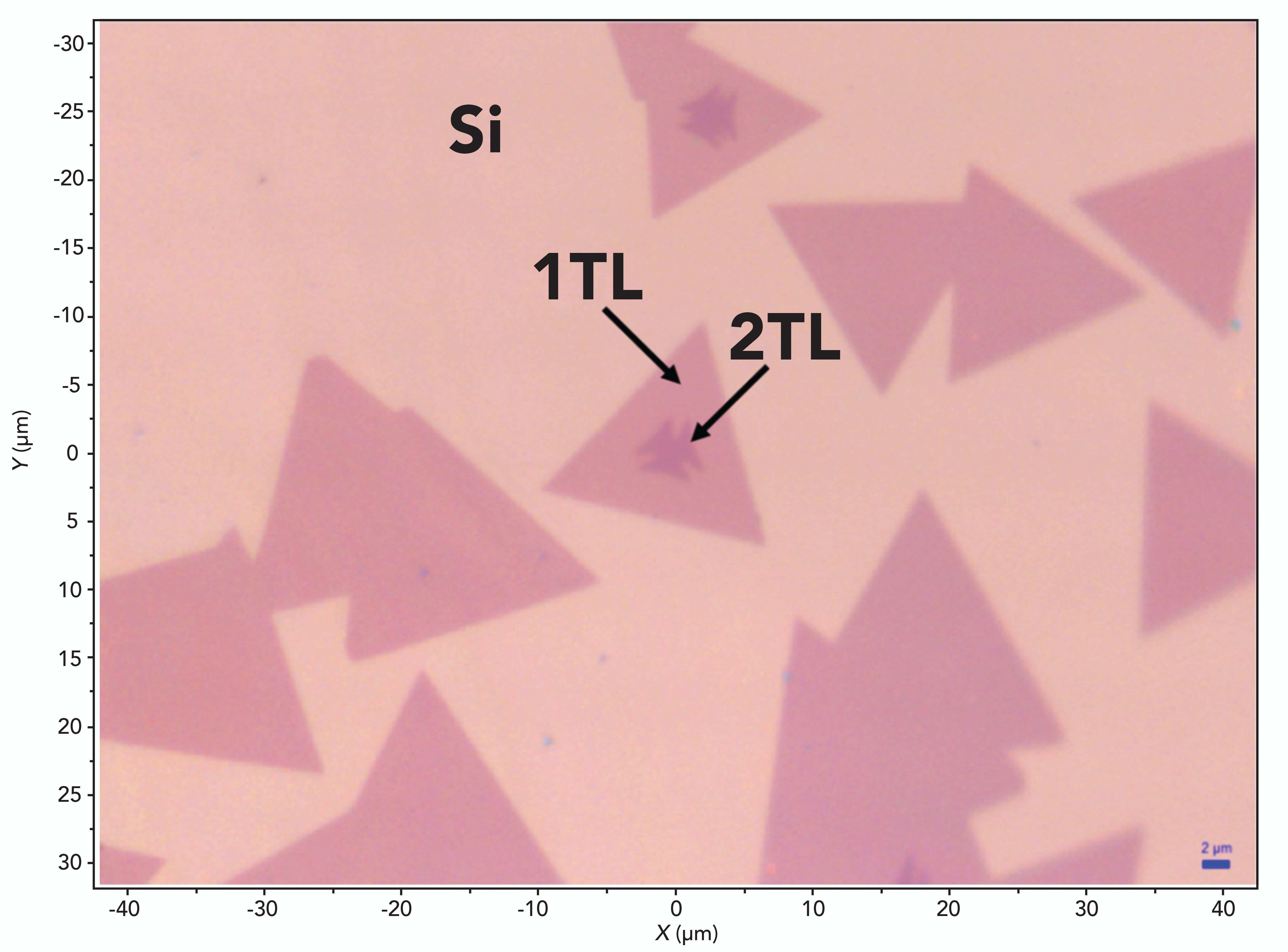
Figure 2: Raman spectra acquired from the light pink (blue spectrum) and dark pink (red spectrum) areas shown in Figure 1.
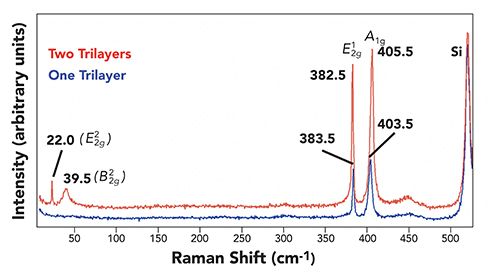
Here, we address our assignment of the low-energy Raman bands, and do so following the work of Zhang and coworkers on shear and interlayer breathing modes of MoS2 (5). The crystals with odd numbers of trilayers belong to crystal class D3h, whereas those with even numbers of trilayers belong to D6h. The Zhang calculations, based on a diatomic chain model (DCM), predict a Raman active B22g mode at 23 cm-1, and a silent mode at 40 cm-1 for a 2D MoS2 crystal consisting of two trilayers. Although the B22g mode is silent, Zhang and coworkers state that “the Raman inactive layer breathing modes (LBMs) (B22g) in even number layered MoS2 might be observed, with polarization behavior identical to the A’1 (LBMs) in odd number layered MoS2” (5). Therefore, based on the appearance of bands at 22.0 cm-1 and 39.5 cm-1 in the spectrum of the dark pink region, in agreement with those calculated by Zhang and coworkers for the double trilayer crystal, we assign them to E22g and B22g, respectively. The absence and appearance of these low-energy bands, along with the increasing separation between the E12g and A1g bands of MoS2 from 20.0 cm-1 to 23.0 cm-1 in the spectra of light and dark pink regions, is consistent with the Zhang calculations for single and double trilayers, respectively.
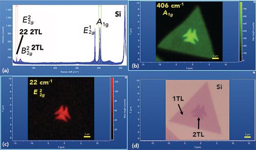
Raman imaging further supports the layer number assignment of the light and dark pink regions. A collection of hyperspectral data and corresponding Raman images acquired from the central 2D MoS2 crystal of Figure 1 are shown in Figure 3. A reflected white light image of the crystal appears in the lower right hand corner, and corresponding 406 cm-1 (A1g) and 22 cm-1 (E22g) Raman images appear above and to the left of the reflected light image, respectively. The plot on the upper left consists of all of the Raman spectra acquired over the image area. The Raman data were acquired using 532 nm excitation and a 100X Olympus objective, and by moving the stage in 400 nm increments over an area of approximately 19 µm x 19 µm. The Raman images are rendered from the spatial variation of the Raman intensity within the color coded brackets shown in the hyperspectral data set in the upper left hand corner. The red and green brackets are centered on 22 cm-1 and 406 cm-1, respectively. The differences in the signal strengths related to the number of trilayers can be clearly seen in the Raman image of the 406 cm-1 (A1g) band shown in Figure 3. That portion of the 406 cm-1 (A1g) band Raman image corresponding to the dark pink region is approximately twice as bright as the surrounding triangle of MoS2. The association of that increased signal strength with the double trilayer is confirmed by the correspondence to, and registration with, the Raman image rendered from the mapping of the interlayer shear mode band signal strength at 22 cm-1.
Figure 3: (a) Raman spectra and images acquired from the (b) single (1TL) and (c) double (2TL) trilayer areas as shown in (d) and in Figure 1.
Crystals with three trilayers exhibit the same optical and spectral trends observed in progressing from a single to a double trilayer. A reflected white light image consisting of the Si substrate and 2D MoS2, with single (1TL), double (2TL) and triple (3TL) trilayers, is shown in Figure 4. The single trilayer MoS2 appears light pink, and the double and triple trilayers appear progressively darker. The dark triangle in the center of the image is a triple trilayer. Raman spectra acquired from the areas with one, two, and three trilayers are shown in Figure 5. The single trilayer spectrum consists of the Si substrate Raman band and only the and A1g bands at higher energy. The absence of the low-energy E22g and B22g bands confirms that the crystal in that location consists of only a single trilayer. The Raman spectrum from the double trilayer region consists of the Si substrate Raman band, the high-energy E12g and A1g bands, and two low-energy bands which we attribute to the shear (E22g) and interlayer breathing modes (B22g). The spectrum obtained from the triple trilayer triangle in the center of Figure 4 consists of the four bands that appear in the double trilayer spectrum. However, both low-energy bands are noticeably shifted to lower energy, and are assigned new symmetry species E” and A’1 commensurate with the change to the D3h crystal class for odd trilayer MoS2. These same spectra are plotted on an expanded scale in Figure 6. The E12g and A1g bands at higher energy manifest increasing band separation with trilayer number progressing from 20.5 cm-1 to 23.5 cm-1 to 25.0 cm-1 for the single, double, and triple trilayers, respectively.
Figure 4: Reflected white light image of 2D MoS2 with single (1TL), double (2TL) and triple (3TL) trilayers prepared by chemical vapor deposition on a Si substrate.
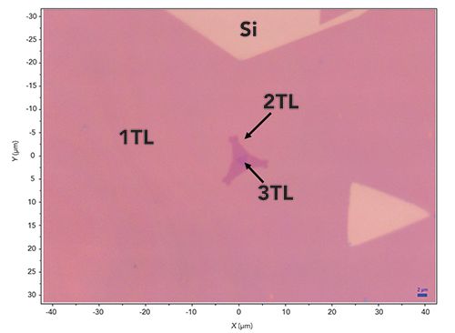
Figure 5: Raman spectra acquired from the single (blue), double (red) and triple (green) trilayer areas shown in Figure 4.
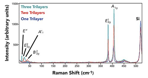
Figure 6: Raman spectra acquired from the single (blue), double (red) and triple (green) trilayer areas as shown in Figure 4.
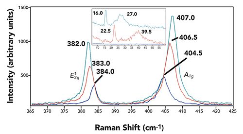
The inset of the plot in Figure 6 shows an expanded scale of the low-energy region of the spectrum. The double trilayer spectrum with bands at 22.5 cm-1 and 39.5 cm-1 is in good agreement with that shown in Figure 2. The triple trilayer spectrum has low-energy bands; however, they have shifted to 16.0 cm-1 and 27.0 cm-1, respectively. These experimental results are in good agreement with those values calculated based upon the diatomic chain model (DCM) (5). The experimentally obtained results along with the DCM expectations calculated by Zhang and coworkers are shown in Table I.

In summary, we can conclude that the low-energy band positions are consistent with and provide the same information regarding the number of trilayers as does the higher energy E12g and A1g band separation for few-layer MoS2. Nevertheless, the low-energy band positions change to a greater extent than does the higher energy E12g and A1g band separation and are therefore more sensitive to the number of trilayers in 2D MoS2.
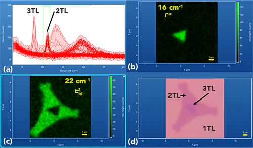
The distinction between the double and triple trilayers and correspondence to the reflected white light image can be seen in the 22.0 cm-1 and 16.0 cm-1 Raman images shown in Figure 7. A reflected white light image of the crystal appears in the lower right hand corner and corresponding 16.0 cm-1 (E”) and 22.0 cm-1 (E22g) Raman images appear above and to the left of the reflected light image, respectively. The plot on the upper left consists of all of the Raman spectra acquired over the image area. The Raman data were acquired using 532 nm excitation and a 100X Olympus objective and by moving the stage in 300 nm increments over an area of approximately 13 µm x 13 µm. The 22.0 cm-1 band intensity attributed to the double trilayer is appreciable only in the three-pronged structure and is absent in the single and triple trilayer areas. The 16.0 cm-1 band appears only in the triangle at the center, the triple trilayer. These images demonstrate how Raman imaging in the low-energy region of the spectrum can readily be used to reveal the spatial variation of the single, double and triple trilayers in MoS2.
Figure 7: (a) Raman spectra and images acquired from single, (c) double (2TL at 22 cm-1), and (b) triple (3TL at 16 cm-1) trilayer areas as shown in (d) and in Figure 4.
Crystal Stacking Orientation and Low-Energy Band Position
The interpretation of the Raman spectra in the low-frequency region is made complex by the different symmetry species of the low-energy vibrational modes for odd and even numbers of trilayers (5–9). Furthermore, other reports have shown how stacking orientation can affect interlayer coupling and therefore the positions of the low-energy bands arising from shear and interlayer breathing modes (10–12). We discuss here how the progression of the shear and interlayer breathing modes’ peak positions and signal strengths depend upon the parallel or anti-parallel layer orientation as the number of trilayers increase.
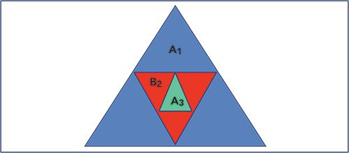
To facilitate the discussion of spectra obtained from 2D crystals of MoS2 with parallel or anti-parallel stacking of crystal layers, we use the labeling system described in Figure 8. The graphic depicts a three trilayer crystal of order and orientation A1B2A3. The first trilayer (1) on the substrate is pointed upwards (A) and so we designate that trilayer A1. If the second trilayer (2) on top of the first trilayer is pointed downwards (B), we designate that trilayer B2. A third trilayer (3) on top of the second trilayer that is pointed upwards is designated A3, and so on.
Figure 8: Labeling system and graphic of 2D Si substrate crystal few-layer orientation. The graphic depicts a three trilayer crystal of order and orientation A1B2A3, where the first large blue A1 is on the Si substrate, the red B2 is on top of blue A1, and the green A3 is on top of red B2.
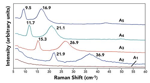
A reflected white light image of a five trilayer A1A2A3A4A5 oriented 2D MoS2 crystal on a Si substrate is shown in Figure 9. Raman spectra obtained from an exposed portion of each level of the trilayers are shown in Figure 10. The intensity scale of the spectra in Figure 10 has been set to more clearly view the progressive shift of the low-energy shear mode (SM) and interlayer breathing mode (BM) bands to lower wavenumbers with increasing trilayer number. Although one cannot see it in Figure 10, the higher energy E12g and A1g band separation increases with each additional trilayer (17.7 cm-1 [A1], 21.5 cm-1 [A2], 25.5 cm-1 [A3], 25.7 cm-1 [A4], and 25.9 cm-1 [A5]). This band separation is commonly used to determine the number of trilayers in the 2D crystal. However, we see again that the low-energy shear mode and interlayer breathing mode band positions are more sensitive to the number of trilayers, particularly beyond three trilayers. An expanded scale plot of these same spectra is shown in Figure 11 wherein the low-energy peak positions are labeled. Note that both the shear and interlayer breathing modes move progressively to lower energy with increasing trilayer number. Furthermore, the intensities of the shear and interlayer breathing modes remain fairly constant relative to those of the higher energy E12g and A1g bands. Therefore, we can conclude that the interlayer bond polarizabilities do not substantially increase with increasing trilayer number in the A1A2A3A4A5 parallel oriented 2D MoS2.
Figure 9: Reflected white light image of a five trilayer A1A2A3A4A5 oriented 2D MoS2 crystal prepared by chemical vapor deposition on a Si substrate.
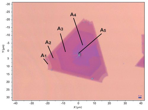
Figure 10: Raman spectra highlighting the shear mode (SM) and interlayer breathing mode (BM) of one (A1), two (A2), three (A3), four (A4) and five (A5) trilayer locations in the A1A2A3A4A5 oriented 2D MoS2 crystal shown in Figure 9.
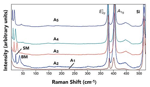
Figure 11: Raman spectra highlighting the shear mode and interlayer breathing mode shifts of one (A1), two (A2), three (A3), four (A4) and five (A5) trilayer locations in the A1A2A3A4A5 oriented 2D MoS2 crystal shown in Figure 9.
An anti-parallel alignment of successive trilayers in oriented 2D MoS2 yields a markedly different progression of the peak positions of the low-energy bands with increasing number of trilayers. A reflected white light image of a four trilayer A1A2B3A4 oriented 2D MoS2 crystal is shown in Figure 12. Raman spectra obtained from an exposed portion of each level of the trilayers are shown in Figure 13. Note how much more intense the shear mode band (21.6 cm-1 in A2) is in the spectra of the anti-parallel A1A2B3A4 oriented form of the 2D MoS2 crystal compared to its counterpart in the A1A2A3A4A5 parallel oriented crystal spectra as seen in Figure 10.
Figure 12: Reflected white light image of a four trilayer A1A2B3A4 oriented 2D MoS2 crystal prepared by chemical vapor deposition on a Si substrate.
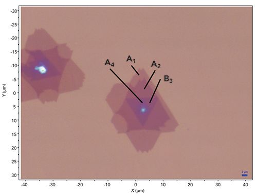
Figure 13: Raman spectra highlighting the shear mode (SM) and interlayer breathing mode (BM) of one (A1), two (A2), three (B3), and four (A4) trilayer locations in the A1A2B3A4 oriented 2D MoS2 crystal shown in Figure 12.
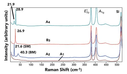
Furthermore, the strength of the shear mode in the third anti-parallel trilayer (26.9 cm-1 in B3) of the A1A2B3A4 oriented MoS2 spectrum is comparable to those of the higher energy E12g and A1g bands in the same spectrum. The increased signal strength of the shear mode band indicates an increase in the interlayer polarizability when the trilayers are oriented anti-parallel with respect to each other. An expanded scale plot of these same spectra is shown in Figure 14 to more clearly see the shifts in the opposite directions of the shear and interlayer breathing mode bands with increasing trilayer number. The peak positions of the two trilayer (A2) shear and interlayer breathing modes at 21.6 cm-1 and 40.3 cm-1 in the A1A2B3A4 oriented crystal spectrum are similar to those of the A1A2A3A4A5 orientation at 21.9 cm-1 and 36.9 cm-1 shown in Figures 14 and 11, respectively. However, the presence of a third trilayer oriented anti-parallel with respect to the first two trilayers in the A1A2B3A4 oriented crystal causes the shear mode to shift from 21.6 cm-1 (A2) to a higher energy at 26.9 cm-1 (B3), whereas the interlayer breathing mode shifts to lower energy just as it does in the A1A2A3A4A5 orientation. In fact, because the shear and interlayer breathing mode bands shift in the opposite direction with anti-parallel orientation, they are now closely spaced and only partially resolved in trilayer B3. The effect of the third layer anti-parallel orientation on the directional shifts of the low-energy bands continues with the fourth trilayer (A4) even though it has the same orientation as that of the first two layers. The shear and interlayer breathing mode peak positions of the fourth trilayer (A4) are 28.9 cm-1 and 21.9 cm-1, respectively. The relative positions of the shear and interlayer breathing mode bands in the A1A2B3A4 oriented crystal spectrum have reversed in progressing from trilayer levels A2 to A4. The principal finding is that the progression of relative peak positions of the shear and interlayer breathing modes in a crystal with anti-parallel trilayer orientation is the opposite of that observed for crystals with parallel trilayer orientation.
Figure 14: Raman spectra highlighting the shear mode and interlayer breathing mode shifts of one (A1), two (A2), three (B3), and four (A4) trilayer locations in the Figure 14: Raman spectra highlighting the shear mode and interlayer breathing mode shifts of one (A1), two (A2), three (B3), and four (A4) trilayer locations in the A1A2B3A4 oriented 2D MoS2 crystal shown in Figure 12.
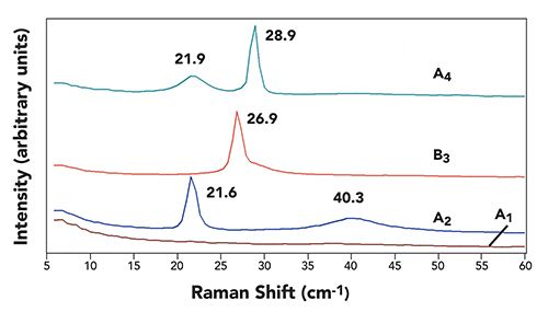
It is important to note that the effects of trilayer orientation extend throughout the 2D crystal, including exposed perimeters of underlying trilayers. Compare the relative signal strengths of the shear and interlayer breathing modes of the two trilayer spectra (A2) in the A1A2A3A4A5 and A1A2B3A4 crystals. Measured at a location at which only the first two trilayers are exposed, one might suppose that the spectra would be the same were the material to be simply a collection of MoS2 trilayers, and not a 2D crystal. The band positions are indeed similar; however, the Raman signal strength of the A2 shear mode band in the A1A2B3A4 crystal spectrum is significantly greater than its counterpart band in the spectrum of the A1A2A3A4A5 crystal. This spectral behavior confirms that the entire material is indeed a 2D crystal with interlayer forces extending beyond trilayer perimeters to exposed levels below.
The spectral results discussed here have important consequences for the characterization of continuous 2D films with no obvious crystal habit revealing the solid-state structure. The combination of reflected white light images with the corresponding Raman spectra of exposed levels can be used to establish reference spectra of the number and stacking orientation of trilayers in 2D MoS2 crystals. The reference low-energy Raman band structure can then reveal the number and orientation of the trilayers in 2D MoS2 even when the reflected white light image of a crystal or extended film may not reveal the number of trilayers or stacking orientation.
Conclusion
We acquired and analyzed Raman spectra of few-layer 2D MoS2 crystals prepared by chemical vapor deposition and consisting of different numbers of trilayers. We observed that the low-energy band positions change to a greater extent than does the separation of higher energy E12g and A1g bands and are therefore more sensitive to the number of trilayers in 2D MoS2. Raman imaging was performed on these crystals and demonstrated how Raman images of the low-energy region of the spectrum reveal the spatial variation of the single, double and triple trilayers in MoS2. Crystals consisting of different stacking orientation were analyzed by Raman spectroscopy. The shear and interlayer breathing modes’ peak positions and signal strengths depend upon the parallel or anti-parallel crystal stacking orientation as the number of trilayers increase. The principal finding is that the progression of relative peak positions of the shear and interlayer breathing modes in a crystal with anti-parallel trilayer orientation is the opposite of that observed for crystals with parallel trilayer orientation.
References
- D. Tuschel, Spectroscopy 30(9), 18–31 (2015).
- D. Jariwala, V.K. Sangwan, L.J Lauhon, T.J. Marks, and M.C. Hersam, ACS Nano 8, 1102–1120 (2014).
- G. Eda and S.A. Maier, ACS Nano 7, 5660–5665 (2013).
- H. Li, J. Wu, X. Huang, G. Lu, J. Yang, X. Lu, Q. Xiong, and H. Zhang, ACS Nano 7, 10344–10353 (2013).
- X. Zhang, W.P. Han, J.B. Wu, S. Milana, Y. Lu, Q.Q. Li, A.C. Ferrari, and P.H. Tan, Phys. Rev. B87, 115413 (2013).
- H. Zeng, B. Zhu, K. Liu, J. Fan, X. Cui, and Q.M. Zhang, Phys. Rev. B 86, 241301(R) (2012).
- L. Liang, J. Zhang, B.G. Sumpter, Q.-H. Tan, P.-H. Tan, and V. Meunier, ACS Nano 11, 11777–11802 (2017).
- X. Zhang, X.F. Qiao, W. Shi, J.B. Wu, D.S. Jiang, and P.H. Tan, Chem. Soc. Rev. 44, 2757–2785 (2015).
- Y. Zhao, X. Luo, H. Li, J. Zhang, P.T. Araujo, C.K. Gan, J. Wu, H. Zhang, S.Y. Quek, M.S. Dresselhaus, and Q. Xiong, Nano Lett.13, 1007–1015 (2013).
- J. Yan, J. Xia, X. Wang, L. Liu, J.L. Kuo, B.K. Tay, S. Chen, W. Zhou, Z. Liu, and Z.X. Shen, Nano Lett. 15, 8155–8161 (2015).
- M. O’Brien, N. McEvoy, D. Hanlon, T. Hallam, J.N. Coleman, and G.S. Duesberg, Sci. Reports 6, 19476 (2016).
- X. Luo, X. Lu, C. Cong, T. Yu, Q. Xiong, and S.Y. Quek, Sci. Reports 5, 14565 (2015).

David Tuschel is a Raman applications scientist at Horiba Scientific, in Piscataway, New Jersey, where he works with Fran Adar. David is sharing authorship of this column with Fran. He can be reached at: SpectroscopyEdit@MMHGroup.com

AI-Powered SERS Spectroscopy Breakthrough Boosts Safety of Medicinal Food Products
April 16th 2025A new deep learning-enhanced spectroscopic platform—SERSome—developed by researchers in China and Finland, identifies medicinal and edible homologs (MEHs) with 98% accuracy. This innovation could revolutionize safety and quality control in the growing MEH market.
New Raman Spectroscopy Method Enhances Real-Time Monitoring Across Fermentation Processes
April 15th 2025Researchers at Delft University of Technology have developed a novel method using single compound spectra to enhance the transferability and accuracy of Raman spectroscopy models for real-time fermentation monitoring.
Nanometer-Scale Studies Using Tip Enhanced Raman Spectroscopy
February 8th 2013Volker Deckert, the winner of the 2013 Charles Mann Award, is advancing the use of tip enhanced Raman spectroscopy (TERS) to push the lateral resolution of vibrational spectroscopy well below the Abbe limit, to achieve single-molecule sensitivity. Because the tip can be moved with sub-nanometer precision, structural information with unmatched spatial resolution can be achieved without the need of specific labels.