GC-ICP-MS for Process and Quality Control in Semiconductor Manufacturing
Gas chromatography (GC) coupled to inductively coupled plasma–mass spectrometry (ICP-MS) is a powerful and flexible analytical solution that is well-established for measuring organometallic compounds such as organotin, organomercury, and organolead in environmental samples, foodstuffs, and consumer products. GC–ICP-MS is also used for industrial applications, such as monitoring catalyst poisons and environmental contaminant elements in petrochemical processing and plastics manufacturing. The semiconductor industry uses a range of high-purity specialty gases and volatile liquids as precursors in wafer substrate production, and for processes such as plasma etching and deposition of thin films by chemical vapor deposition (CVD). Semiconductor manufacturers are constantly developing new integrated circuit (IC) chips with smaller sizes, higher speeds, lower power consumptions, and greater transistor densities. This trend means that contaminants must be controlled at even lower levels in process chemicals and precursors. In this article, we show how GC–ICP-MS, particularly using triple quadrupole or tandem ICP-MS (ICP-MS/MS), enables determination of the lowest levels of contaminants in the specialty gases and volatile liquids used to make the most advanced electronic devices.
Integrated circuit (IC) chips play an increasingly important role in modern life, supporting technologies from consumer electronics and self-driving vehicles to the high-speed communications and servers used in accelerated computing and artificial intelligence (AI). The manufacturing of advanced semiconductor chips requires high-purity materials, metals, and a range of process chemicals, such as ultrapure acids and solvents. Wafer manufacturers and chip fabrication plants (FABs) also use a variety of bulk and electronic specialty gases (ESGs) and volatile liquids throughout the manufacturing process (1,2). For example, silane (SiH4) and chlorosilanes are used as feedstocks for gas purification of silicon to the nine to eleven nines purity used to make semiconductor wafers. Nine nines (9N) Si is 99.9999999% pure, meaning there is only 1 part per billion (ppb) of total impurity elements in the solid silicon crystal. Alternative, non-silicon wafers and films are often made from “III-V compound” semiconductors, such as gallium arsenide (GaAs) and indium GaAs (InGaAs), which may use arsine gas (AsH3) as a precursor together with trimethyl gallium (TMG).
Fabricating an advanced IC chip involves upwards of a thousand steps where thin layers of conducting and insulating material are alternately deposited and etched to create the millions of transistors and other features that make up the circuit. Dopant elements are added to modify the conductivity of the silicon substrate or surface film. High-purity gases are used extensively in these “front end” IC fabrication processes. For example, phosphine (PH3) is used to dope the required level of phosphorus into thin-film transistor (TFT) displays. Diborane (B2H6) is used for boron doping and ion implantation, for growing metal-boron thin films, and as a component of chemical vapor deposition (CVD) of boron-phosphate-silicate-glass (BPSG) films. Fluorocarbon (FC) gases, such as 2-fluorobutane and hexafluoro butadiene, are also used in the electronics industry (for example, in dry etching and for plasma enhanced chemical vapor deposition [PECVD]). The high reactivity and low toxicity of some FC gases means they are also used to clean reaction chambers between fabrication processes. In a typical semiconductor FAB, high-purity gases can make up the second largest material cost after high-purity silicon.
Controlling the level of contaminants in specialty gases is critical to ensuring acceptable chip yield and the performance and reliability of the finished semiconductor device. To understand why contamination is so important, it is useful to consider that advances in semiconductor device technology are driven by reductions in scale. Packing more transistors into a smaller space improves the speed and performance of the chip. The latest chips have circuit features and line widths measured in single nanometers (nm, one millionth of a millimeter), and the presence and position of individual atoms in the silicon crystal lattice can affect the electrical properties of the device. This makes the chips highly susceptible to contamination, so controlling the levels of impurities in the high-purity gases used during fabrication is fundamental to the production process.
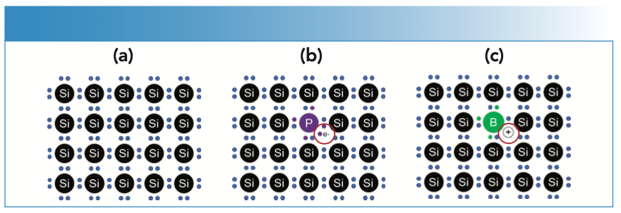
Controlling the levels of dopant elements and metallic contaminants in substrate materials, process chemicals, and gases, is a particular industry concern. Dopant elements are deliberately added to the silicon substrate to make it “semiconducting” and control the electrical properties, as illustrated in Figure 1. Silicon has four valence electrons, and pure silicon forms a crystal lattice in which all these electrons are shared with the adjacent silicon atoms. As a result, pure silicon is a poor conductor of electricity. N-type (negative) dopants are Group V elements such as phosphorus, arsenic, antimony, and bismuth, which have five valence electrons, so they add one free electron to the silicon lattice. P-type (positive) dopants are Group III elements, which have three valence electrons, so they contribute a “missing” electron or a positive “hole” in the lattice. The level of doping varies depending on the intended properties, but low-level doping can add as few as one dopant atom per 100 million silicon atoms, so controlling contamination for these elements is critical.
FIGURE 1: Schematic showing: (a) Pure silicon crystal lattice; (b) silicon doped with phosphorus, an n-type dopant element; (c) silicon doped with boron, a p-type dopant element.
ICP-MS instruments are already widely used in the semiconductor industry to monitor the levels of ultratrace contaminants in high-purity materials and process chemicals. Contaminants in high-purity gases often need to be controlled at lower levels than can be achieved using traditional gas chromatography (GC) detectors, which may not have sufficient selectivity for the required analysis to begin with. Also, for some matrices and compounds, standards are unstable or not available, making calibrating and quantifying contaminants difficult.
As a detector for GC, ICP-MS, particularly with a triple quadrupole or tandem mass spectrometer (MS/MS), can overcome many of the limitations of other GC detectors. GC–ICP-MS can detect and quantify almost every element at low levels in gases and volatile liquids. The technique gives element and isotope-specific analysis, and is highly selective. As a result, matrix components and other compounds have little to no impact on the signal for the target analyte. GC–ICP-MS also gives practically the same elemental signal regardless of the compound, so non-specific or “compound independent” calibration (CIC) can be used, simplifying the quantification of compounds that are unstable or for which standards are not available. GC–ICP-MS is a versatile and sensitive technique that enables semiconductor manufacturers to reliably quantify trace-level contaminants in the wide range of specialty gases and volatile liquids used in semiconductor manufacturing.
Experimental
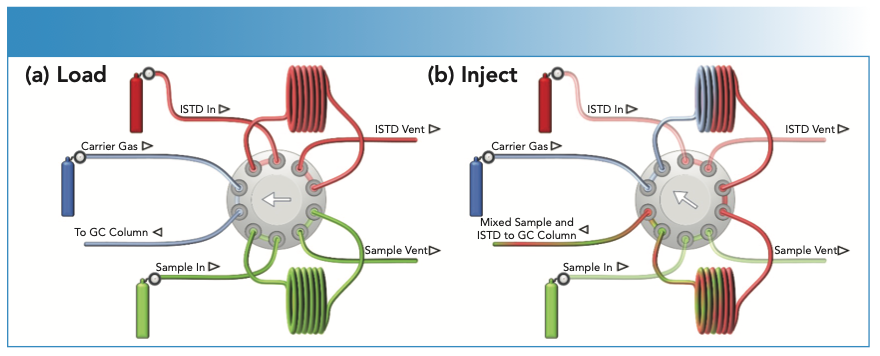
Examples of different electronic gas analysis applications are presented in this work. The details of the specific GC columns and methods used for the different sample types and compounds measured are provided in the discussion. Specialty electronic gas analysis using GC–ICP-MS often requires a special approach to sample introduction and analysis, as many of the gases are toxic, flammable, and pyrophoric (spontaneously combust on contact with air or moisture). Silicon compounds such as silanes, siloxanes, and chlorosilanes decompose to form silica, which would deposit in a standard GC injector. Flammable and pyrophoric gases can be analyzed directly from the cylinder, using a switch- ing valve and loop to deliver the required sample volume directly to the column in the GC injector port. A 10-port sampling valve provides the option to automatically add a second gas as an online internal standard, as illustrated in Figure 2. In a similar way, volatile liquids such as trichlorosilane (TCS) can be sampled and injected directly into the GC–ICP-MS system using a high-pressure switching valve (3).
FIGURE 2: Direct sampling of flammable and pyrophoric gases for analysis by GC–ICP-MS, using a 10-port valve to allow online addition of an internal standard to the sample gas. Showing the (a) load and (b) inject sequences.
A further consideration when GC– ICP-MS is used to analyze samples such as silanes, chlorosilanes, AsH3, PH3, and germane (GeH4) is that these compounds are inorganic. This means the matrix is not easily decomposed and volatilized in the ICP instrument, unlike with hydrocarbon matrices. To successfully analyze these inorganic matrices, a low-volume Deans Switch microfluidic flow control device was used to divert the matrix to vent, preventing excessive matrix load from reaching the ICP. The Deans Switch was positioned in the GC oven in the flow path between the column exit and the ICP-MS transfer line. Once the retention time of the matrix peaks were established using a low volume injection, the Deans Switch was used to divert the matrix to vent during the GC separation.
Both single and triple quadrupole (QQQ) Agilent ICP-MS systems were used for elemental detection. ICP-QQQ is a tandem MS configuration (MS/MS); as a result, it supports the use of reactive cell gases to give more effective control of spectral overlaps. In many cases, analysis can be performed on either type of mass spectrometer, with ICP-MS/MS typically giving detection limits (DLs) that are approximately an order of magnitude lower or more, depending on the element. Because the ICP-MS plasma is “dry” (no aqueous solution), many spectral backgrounds are much lower with GC–ICP-MS than with the conventional liquid sample introduction. As a result, non-typical ICP-MS elements, such as silicon and sulfur, can be measured at their major isotopes using single quadrupole ICP-MS. However, lower DLs are possible if an ICP-MS/MS method is used with a reactive cell gas to further reduce spectral overlaps. For more typical ICP-MS elements, such as germanium and arsenic, part per trillion (ppt) level DLs are routinely achievable. As a multi-element detector, GC–ICP-MS can be used to analyze hydride gas contaminants such as SiH4, PH3, AsH3, and GeH4 at trace level (single ppb down to 10 ppt DLs) in other ultrapure hydride gases (4).
Results and Discussion
Trace Sulfur Compounds in Phosphine
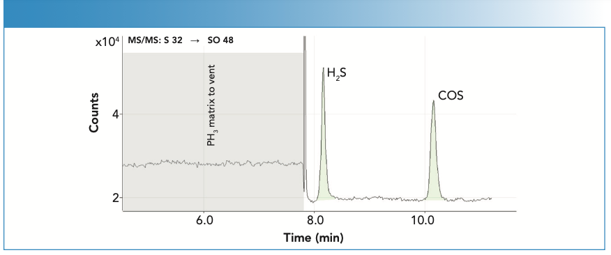
The sulfur compounds, hydrogen sulfide (H2S) and carbonyl sulfide (COS), were determined as ppb-level contaminants in PH3 using a 60-m (2 x 30 m) x 0.53 mm i.d. x 20 μm film mega-bore Plot U GC column at 50 oC with helium carrier gas at 17.5 psig. Sulfur was measured as the 32SO+ product ion using ICP-MS/MS with O2 cell gas and mass shift mode (Q1 (m/z 32) → Q2 (m/z 48)), to avoid any overlap from the 31P matrix peak. The chromatogram is illustrated in Figure 3, demonstrating the complete separation of the sulfur compounds from the PH3 gas. The shaded region of the time plot shows when the PH3 matrix was diverted to vent using the Deans Switch.
FIGURE 3: GC–ICP-MS/MS analysis of trace sulfur compounds in phosphine (PH3). Deans Switch diverts PH3 matrix to vent, avoiding excessive matrix loading to the ICP. Sulfur compounds at 25 ppb each. ICP-MS/MS compound DLs were approximately 1.5 ppb.
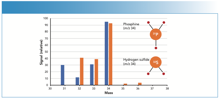
Measurement of H2S in a PH3 matrix is difficult for organic MS as the two compounds both have their large molecular ion peak at m/z 34 and their fragmentation patterns are similar. As illustrated in Figure 4, the only major difference in the GC–TOF-MS spectra is the 31P peak at m/z 31, which is not useful for quantifying sulfur. Although H2S is separated from the PH3 matrix peak chromatographically, the tail of the matrix peak causes a raised background for H2S. By contrast, low-level determination of H2S in a PH3 matrix is straightforward using ICP-MS, which is a mass-specific elemental detector that determines 32S free from any overlap from 31P.
FIGURE 4: H2S mass spectrum is overlapped by PH3 when measured by GC–TOF-MS. Mass-specific elemental detection of 32S by ICP-MS/MS avoids overlap from 31P, enabling interference-free, trace-level analysis of H2S and COS (shown in Figure 3).
Trace Phosphine in Dichlorosilane
As discussed above, PH3 is a critical high-purity process gas, in which sulfur compounds and other hydride contaminants must be monitored at trace levels. However, PH3 also needs to be measured as a trace-level contaminant in other gases and volatile liquids used in the semiconductor industry, to avoid unwanted contamination by phosphorus, an n-type dopant element. Dichlorosilane (DCS) is used as a precursor for high-purity silicon crystal growth, and in combination with ammonia (NH3) to grow silicon nitride (SiN) thin films by CVD. The purity of the silicon crystal or SiN film depends on the purity of the precursor gases, so contaminants including PH3 must be monitored at ppb levels in the DCS. PH3 was determined in DCS by GC–ICP-MS/MS using a 60 m x 0.32 mm x 5.0 μm film DB-1 column using helium carrier gas at 20 psig. The oven program had a starting temperature of 35 oC with a 15 oC/min ramp and a final temperature of 220 oC.
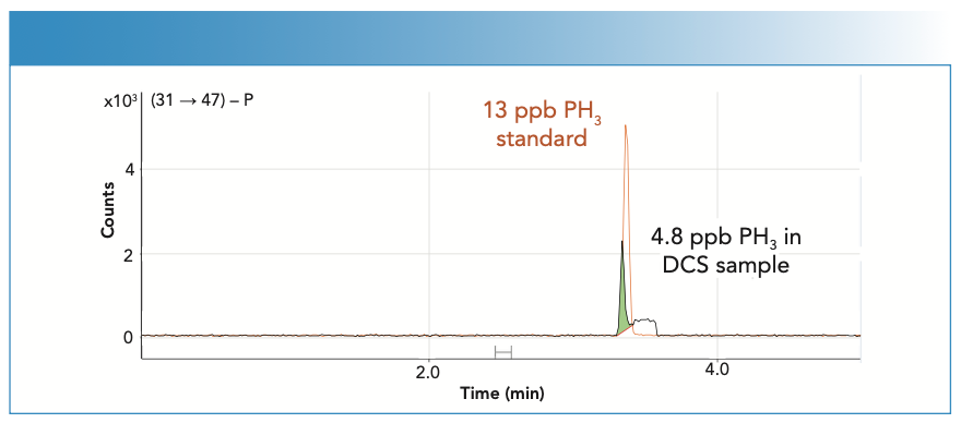
Figure 5 shows overlaid chromatograms for a PH3 standard at 13 ppb and PH3 being determined as a trace contaminant in DCS. The PH3 contaminant was quantified at 4.8 ppb. The use of ICP-MS/MS with O2 cell gas and mass shift mode (Q1 [m/z 31] → Q2 [m/z 47]) enabled low-level phosphorus analysis with minimal contribution from the silicon matrix.
FIGURE 5: Overlaid GC–ICP-QQQ chromatograms showing trace PH3 contaminant quantified at 4.8 ppb in DCS matrix, overlaid with PH3 standard (13 ppb).
Higher Borane Contaminants in Diborane
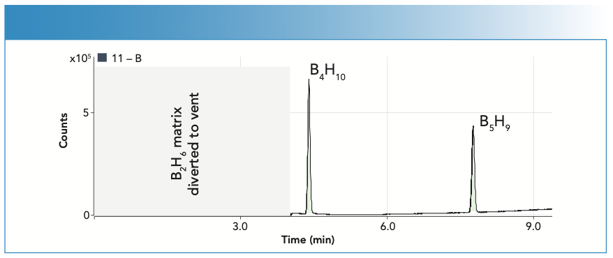
GC–ICP-MS was used to measure higher boranes as trace impurities in high-purity diborane (B2H6) using a 60 m x 0.32 mm x 1.5 m Rtx-Volatiles column. The oven program used a 35 oC starting temperature with a 15 oC/min ramp and a final temperature of 240 oC. Tolerances for diborane purity are extremely tight (<1% variation), so accurate measurement of higher boranes is essential for production control. Standards are not available or stable for higher boranes, but GC–ICP-MS provides a solution, as illustrated in Figure 6. The chromatogram shows the separation and quantification of tetraborane (B4H10) and pentaborane (B5H9) in a B2H6 matrix. The higher boranes were quantified at single ppm levels in 2% B2H6 using CIC against a diborane standard. Quantification by CIC is based on the consistent response for elemental boron and a simple mathematical correction for the different amounts of boron in the different compounds. ICP-MS also offers isotope specific measurement, which is beneficial in this application, as some uses of borane require B2H6 that is isotopically enriched up to 99.99% B-11. The 11B/10B isotopic abundances can easily be measured using GC–ICP-MS.
FIGURE 6: Tetra and pentaborane quantified at single ppm levels in 2% B2H6 sample using compound independent calibration with B2H6 standard.
Conclusions
ICP-MS and ICP-QQQ are well-established techniques that are widely used in the semiconductor industry for measuring ultratrace levels of elemental contaminants in wafer substrate materials, metals, and process chemicals. Combining ICP-MS with GC extends the use of the technique to monitoring contaminants in bulk, specialty gases, and volatile liquids. These sample types require special GC sampling approaches, as many of the samples are toxic, flammable, or pyrophoric. Such samples can be handled safely using an appropriate switching valve or loop injection gas sampling system.
As a sensitive, multi-elemental detector for GC, ICP-MS gives low detection limits, mass-specific measurements, and excellent selectivity. GC coupled to a triple quadrupole ICP-MS system enables trace-level analysis of compounds containing elements traditionally considered difficult to determine by ICP-MS, such as silicon and phosphorus. The high temperature of the ICP ion source means that ICP-MS gives nearly equal elemental response regardless of the compound’s composition. This enables the use of compound independent calibration, which is useful when compound-specific calibration standards are unstable or unavailable.
References
(1) Geiger, W. M.; Raynor, M. W.; Eds., Trace Analysis of Specialty and Electronic Gases; John Wiley & Sons Inc., 2013.
(2) Linde. Electronic Special Gases Index. https://www.linde.com/ (accessed 2023-07-01)
(3) Firor, R. L.; Zuo, N. High-Pressure Liquid Injection Device for Agilent Gas Chromatographs; Agilent publication 5989-6081EN, 2008.
(4) Geiger, W. M.; McElmurry, B.; Anguiano, J.; Kelinske, M. Determination of Trace Impurities in Electronic Grade Arsine by GC-ICP-QQQ; Agilent publication 5994-2213EN, 2020.
William M. Geiger is with Consolidated Sciences (CONSCI) Ltd., in Pasadena, Texas. Ed McCurdy and Mark Kelinske are with Agilent Technologies, Inc. Direct correspondence to Ed McCurdy at ed_mccurdy@agilent.com ●
High-Speed Laser MS for Precise, Prep-Free Environmental Particle Tracking
April 21st 2025Scientists at Oak Ridge National Laboratory have demonstrated that a fast, laser-based mass spectrometry method—LA-ICP-TOF-MS—can accurately detect and identify airborne environmental particles, including toxic metal particles like ruthenium, without the need for complex sample preparation. The work offers a breakthrough in rapid, high-resolution analysis of environmental pollutants.
Microplastics Widespread on Catalan Beaches, Study Finds
March 28th 2025In a recent study published in Marine Pollution Bulletin, a team of researchers from several Spain and Portugal universities and institutions (Rovira i Virgili University, Universitat de Barcelona, University of Porto, and Institut d'Investigació Sanitaria Pere Virgili (IISPV) assessed microplastic (MP) contamination along the Mediterranean coastline.
