Reliable Substrate Technology for Surface-Enhanced Raman Spectroscopy
Special Issues
The acquisition of Raman spectra can be eased greatly through the use of surface-enhanced Raman spectroscopy (SERS). In this article, the authors discuss a new substrate technology that delivers reliable and consistent surface enhancement.
Raman spectroscopy has proven to be a very powerful and broadly available tool for biochemical, clinical, and forensic fields. The Raman signal picked up from molecular species results from vibrational resonances, giving rise to a characteristic series of spectral lines shifted away from the excitation wavelength. A more widespread implementation is hampered, however, by a single aspect of Raman spectroscopy, namely, the fairly weak signals generally observed. Several technical achievements have been responsible for easing this problem, including high performance optical filtering, high power excitation, and low noise optical detection. Even so, none of these offer the potential promised by surface-enhanced Raman spectroscopy (SERS).
SERS describes a widely used process by which the normally low level of Raman signal from probe molecules is significantly increased (enhanced). With reports in the literature of up to 15 orders of magnitude signal enhancement, and even with more generally accepted enhancements of a million-fold, the potential for SERS to ease the acquisition of Raman spectra is immense (1, 2).
The physical mechanism for SERS generally is attributed to plasmon localization at "sharp" surface features, with previous surface methodologies having relied upon roughened gold or silver surfaces, gold or silver colloidal media, and more recently, nanotechnology. These approaches have, however, been fraught with poor consistency of the SERS signal. The consequence of this is that, although SERS remains popular for research applications, the commercialization of the technique as a whole has remained difficult to realize.
Ordered, metal-coated nanostructures on a silicon wafer, designed specifically to optimize the plasmon effect and produced using cost-effective wafer-fab techniques, are seen to solve these issues entirely. The degree of enhancement is measured consistently to be in excess of six orders of magnitude, making SERS as simple and as reliable as measuring fluorescence spectra. In this article, we briefly discuss the physics involved, illustrate typical data and repeatability, and discuss the relevance for various applications as well as for Raman instrumentation.
SERS
The concept of surface-enhanced Raman spectroscopy was discovered 30 years ago in Southampton, UK (3). In general, SERS requires the close proximity of, or adsorption by, a microscopically rough metal surface to induce a significant enhancement of the Raman back-scatter from molecules. Solutions or suspensions placed on a rough surface, or molecular gases allowed to contaminate the surface, can exhibit characteristic and significantly enhanced (amplified) Raman spectra. Nonetheless, the homogeneity of this value measured over the surface is general very poor.
The physics of this process is not entirely understood, although it generally has been accepted to be due to surface and localized plasmon resonances, effectively trapping photons and increasing the Raman scattering with vibrational excitations of neighboring molecules (see Figure 1). Favorable metals typically are silver, gold, or platinum, all of which are environmentally stable and possess a high dielectric coefficient (ε1) (the latter translates to a high confinement of light within the metal, necessary for the formation of plasmons within the active surface). In general, silver shows much higher SERS performance than gold, but is subject to slow oxidization in air with subsequent SERS degradation and shorter shelf-life.

Figure 1. Schematic illustrating the SERS process - the surface plasmons serve as a transport mechanism for photons to and from molecules.
More recent approaches have included micro- or nanoscale "roughening," either in the form of electrochemical texturing of a surface before metal sputtering (4), as a metal colloid bonded to a surface (5, 6), or as a metal colloid in close proximity to a surface. This last technique places sample molecules onto a sol-gel matrix of silver particles coating the inside of a glass vial — the molecules are introduced to the vial in solution, permitting SERS of those which then leave solution and embed themselves in the matrix.
Nanoscale approaches have included (self-)assemblies of latex nanoparticles, which, when electroplated and subsequently dissolved away, leave behind nanovoids or nanoholes (ordered and irregular, respectively) (7, 8). The straightforward binding of molecules to single metal nanoparticles also has yielded Raman signal enhancement, leading to the detection of single molecule Raman spectra (1, 2, 9,10). In general, reported signal enhancements are as much as six orders of magnitude or more.
Significantly, none of these technologies have reached a sizeable level of commercial success. Even though the more complex structures exhibit considerable long-range order (the indication being that the manufacture of such surfaces should perhaps be fairly reliable), the level of enhancement measured across a single surface remains unacceptably inconsistent. Enhancement only is observed at so-called "hot spots," regions where the Raman signal is very high, while neighboring regions might exhibit little or even no significant signal enhancement. This situation is exacerbated further by an inconsistency of performance between different but essentially identical substrates. These two aspects together effectively have prevented SERS from being widely recognized as a quantifiable technique.
Ordered Nanostructures
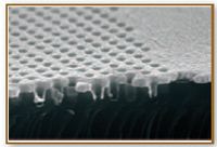
Highly or quasi-ordered nanoscale structures fashioned on a silicon wafer, designed specifically to utilize and optimize the plasmon effect, are seen to solve these issues entirely. These dielectric structures comprise 2D arrays of holes prepared on a silicon wafer surface. Subsequent deposition of a metal surface on to the structured surface gives rise to the desired plasmon effect described earlier (see Figure 2).

Figure 2. Section of an etched photonic crystal surface, coated for use in SERS.
This approach takes its lead from photonic crystal technology — that is, the use of (quasi) periodic 2D or 3D lattices to achieve photonic band structures, in many ways similar to the physics governing the electron band structure in materials. In general, typical optical devices demonstrate photonic band gaps, exceptionally high dispersion, so-called super-prism operation, and wide continuum generation, as well as spectral and spatial filtering (beam shaping) properties (11-14). Proposed applications include components for laser technology, spectrometry, and ultracompact waveguiding.
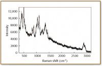
These nanostructured surfaces, appropriately designed specifically for this application and patterned using e-beam lithography, also demonstrate the very high SERS-enhancements reported previously — for some structures consistently greater than six orders of magnitude. Figure 3 illustrates the Raman signal measured from glucose (in solution) placed on one of these substrates. A previous paper on SERS of glucose reports a small Raman cross-section and weak adsorption to metal surfaces (15). Nonetheless, the glucose spectra illustrated here has been quickly and reliably acquired using an absolute minimum of laser intensity and without any partition layers.

Figure 3. Raman spectra of glucose taken via SERS.
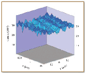
The most critical aspect for commercial applications is the degree of reproducibility seen across a single surface (usually 5 × 5 mm square). Data measured on the 1072 cm-1 benzenethiol Raman peak on a 10-µm raster over an area of 200 by 260 µm illustrate a class minimum of variation in signal enhancement. Furthermore, this homogeneity across a surface is mirrored by moving to all other SERS devices taken from the same wafer, with the additional bonus that the deviation in absolute enhancement is equally small.
Careful modeling and subsequent design indicate that parameters such as the level of enhancement and overall reproducibility both can be tightly controlled. The indications are that features such as shape, depth, and pitch of the holes allow control over the degree of enhancement observed, while aspects such as spatial symmetry of the structure allow control over the level of reproducibility across a surface and is also a principal parameter controlling plasmon dispersion and enhancement.

Figure 4. Consistency data taken on a benzenethiol Raman peak illustrate an rms signal variation of less than 7% (courtesy of Renishaw plc).
Summary
Many other substances that can benefit from the SERS effect show similar enhancements and reproducibility. In addition to glucose, Raman spectra of molecules such as histamine, urea, and phenylalanine have been acquired. These molecules are obtained readily from fluids contained within and on the body, whose levels will all change in relation to different disease processes. Raman spectra of concentrations of these substances down to the micromole level have all been reliably acquired using these SERS substrates. In fact, the lower limit of detection still has to be investigated fully, but these concentrations already are at levels that yield signals below the detection limit for conventional Raman instrumentation.
The manufacture of these substrates involves well-established techniques for silicon wafer fabrication, offering the additional advantage of flexibility in design of the holes and associated structures. This flexibility functions as a design tool during production, allowing the realization of differing structure parameters to achieve different goals. Importantly, the cost-effective nature of the manufacture is critical for what effectively is a "use once" component, as contamination of the surface by a foreign species is measurable readily.
The reproducibility exhibited by these SERS substrates also has significant consequences for Raman instrumentation. In less critical applications, and for many substances that can make use of the SERS effect, the requirements for high laser power, low noise, and highly averaged detection might be superfluous. Additionally, proven reliability of these SERS substrates would enable its recognition as a quantifiable procedure for materials identification or characterization, with significant implications for a range of fields encompassing pharmaceuticals, forensics and trace analysis.
Caterina Netti is research and applications manager, and John Lincoln is director of business development at Mesophotonics Ltd. (UK). E-mail: john.lincoln@mesophotonics.com. Gregory Flinn is a consultant to the photonics industry. E-mail: gregory.flinn@gmx.net
References
1. K. Kneipp, Y. Wang, H. Kneipp, I. Itzkan, R.R. Dasari, and M.S. Feld,
Phys. Rev. Lett.
76
, 2444 (1996).
2. K. Kneipp, Y. Wang, H. Kneipp, L.T. Perelman, I. Itzkan, R.R. Dasari, and M.S. Feld, Phys. Rev. Lett. 78, 1667 (1997).
3. M. Fleischmann, P.J. Hendra, and A.J. McQuillan, Chem. Phys. Lett. 26, 163 (1974).
4. C.A. Murray, D.L. Allara, and M. Rhinewine, Phys. Rev. Lett. 46, 57 (1981).
5. L.A. Dick, A.D. Mcfarland, C.L. Haynes, and R.P. Van Duyne, J. Phys. Chem. B 106, 853-860 (2002).
6. T. Vo-Dinh, Sens. Actuators B 29, 183-189, (1995).
7. M.C. Netti, S. Coyle, J.J. Baumberg, M.A. Ghanem, P.R. Birkin, P.N. Bartlett, D.M. Whittaker, Adv. Mat. 13 1368-1370 (2001).
8. S. Coyle, M.C. Netti, J.J. Baumberg, M.A. Ghanem, P.R. Birkin, P.N. Bartlett, and D.M. Whittaker, Phys. Rev. Lett. 87, 176801 (2001).
9. S. Nie and S. R. Emory, Science 275, 1102 (1997).
10. S.R. Emory and S. Nie, Anal. Chem. 69, 2631 (1997).
11. M.E. Zoorob, M.D.B. Charlton, G.J. Parker, J.J. Baumberg, and M.C. Netti, Nature 404, 740-743 (2000).
12. M.C. Netti, A.D. Harris, J.J. Baumberg, D.M. Whittaker, M.D.B. Charlton, M.E. Zoorob, and G.J Parker, Phys. Rev. Lett. 86, 1526-1529 (2001).
13. M.C. Netti, C.E. Finlayson, J.J. Baumberg, M.D.B. Charlton, M.E. Zoorob, J.S. Wilkinson, and G.J. Parker, Appl. Phys. Lett. 81, 3927 (2002).
14. J.J. Baumberg, N.M.B. Perney, M.C. Netti, M.D.C. Charlton, M. Zoorob, and G.J. Parker, Appl. Phys. Lett. 85, 354 (2004).
15. K.E. Shafer-Peltier, C.L. Haynes, M.R. Glucksberg, and R.P. Van Duyne, J. Am. Chem. Soc. 125, 588-593, (2003).

Tomas Hirschfeld: Prolific Research Chemist, Mentor, Inventor, and Futurist
March 19th 2025In this "Icons of Spectroscopy" column, executive editor Jerome Workman Jr. details how Tomas B. Hirschfeld has made many significant contributions to vibrational spectroscopy and has inspired and mentored many leading scientists of the past several decades.