Combining Confocal Raman with Atomic force Microscopy for High-Resolution Material Analysis
Special Issues
Confocal Raman microscopy can be useful when applied to all samples that are heterogeneous on the micrometer to millimeter scale and that generally can be investigated by Raman spectroscopy. This article presents examples of confocal Raman microscopy from various fields of application including pharmaceutical analysis and stress measurements in semiconductors.
Raman spectroscopy is a well-established, nondestructive analysis technique that delivers detailed chemical information about the molecules involved in the scattering process. Technical samples very often are heterogeneous and the distribution of the compounds is important. However, in most spectroscopy setups, spatial resolution is poor because the exciting laser spot diameter is on the order of 100 µm. In this case, the sample properties are averaged over the size of the laser spot.
Optical microscopy, on the other hand, is capable of providing sub-µm spatial resolution. By integrating a sensitive Raman spectrometer within a state-of-the-art microscope setup, Raman microscopy with a spatial resolution down to 200 nm laterally and 500 nm vertically can be achieved using visible light excitation.
Using the confocal arrangement, in which a pinhole is placed in the focal plane of the microscope to reject out-of-focus light, even depth profiling and 3-D imaging is possible if the sample is transparent. With this technique, it is not only possible to obtain Raman spectra from extremely small sample volumes (down to 0.02 µm3) but also to collect high-resolution Raman images.
In this article, we present examples of confocal Raman microscopy from various fields of application, from pharmaceutical tablets to stress measurements in semiconductors. Please note that these examples are only a limited selection of the enormous variety of possible applications. Confocal Raman microscopy can be useful when applied to all samples that are heterogenous on the micrometer to millimeter scale and that in general can be investigated by Raman spectroscopy.
By adding atomic force microscopy (AFM) to the imaging capabilities, the optical diffraction limit can be overcome and a new dimension in lateral and topographical resolution is achieved. In AFM, the surface topography of a sample is probed with an extremely sharp tip at the end of a small cantilever, delivering nm precision in the lateral, and subnanometer resolution in the vertical dimension.
The topographical structures observed with the AFM then can be linked to and compared with the chemical information obtained by the confocal Raman microscope (CRM). The advantage of combining these techniques in a single instrument is the possibility to switch between the different observation modes with negligible lateral shift. If two separate instruments must be used, finding the same sample position again can be very time consuming, if not impossible without surface markers. One such instrument is available with a special objective that allows the mounting of a cantilever to perform an AFM measurement with highest resolution. Switching between Confocal Raman and AFM is performed by simply rotating the objective turret.
Confocal Raman Microscopy
To obtain a Raman image, the CCD camera of a spectrometer is used to acquire a complete Raman spectrum at a user-defined number of image points per line, while the sample is scanned line by line. The number of image points (spectra) is limited only by the memory of the computer. A typical image consists of 10,000 (100 × 100) to 65,536 (256 × 256) spectra. From this multispectrum file, an image is computed by integrating over a certain Raman line in all spectra. The intensity calculated from each spectrum is color-coded and determines the brightness of the appropriate pixel in the image.
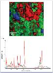
As all spectra are stored in memory, a large variety of properties such as peak-width, center of mass or peak position of certain Raman lines can be calculated from a single measurement and displayed as images. For example, Figure 1a shows the distribution of different components (drug and filler particles) in a pharmaceutical tablet of ASA (acetylsalicyl-acid). The image shows a 200 × 200 µm scan sampled with a resolution of 120 × 120 spectra and an integration time of 70 ms per spectrum. Excitation was performed with a frequency doubled Nd:YAG laser at 532 nm. The drug is color-coded red, while the filler components are shown in green and blue respectively. The spectra of the drug and the filler components are shown in Figure 1b.

Figure 1. (a) Raman spectral image of a pharmaceutical tablet of ASA (acetylsalicylacid). 120 Ã 120 spectra, 70-ms integration time per spectrum. The drug is color coded red, while the filler components are shown in blue and green respectively. (b) Spectra of the drug (ASA, red) and the two filler components (blue and green).
To collect a Raman image in a reasonable amount of time, special care must be taken to optimize the optical throughput and sensitivity of the setup. As a Raman image consists of several thousand pixels (spectra), the integration time per pixel (spectrum) must be as short as possible. As a typical Raman spectral image of 100 lines and 100 pixels per line contains 10,000 spectra, an acquisition time of only 1 s/spectrum results in a total image acquisition time of nearly 3 h, which is not acceptable for routine work.
Increasing the exciting laser power above a few tens of milliwatts to increase the Raman intensity also is not possible usually because sample heating must be avoided. In an optimized setup, the acquisition time per spectrum is typically less than 100 ms for most samples, so that Raman images of 100 × 100 pixels are obtained in little more than 15 min.
In many cases, fluorescence background is no problem because it is either strongly suppressed by the confocal detection scheme or can be very effectively bleached in the focal plane. To obtain this level of resolution and speed, especially with the demand of precision for the AFM in mind, an ultraprecise piezo stage with up to 200 × 200 µm lateral and 20 µm vertical range and capacitive hardware linearization is used for sample scanning.
Confocal Raman-AFM
As nanotechnology is becoming more and more important, there is a growing demand for the characterization of heterogonous systems on the nanometer scale. However, certain properties are difficult to study with conventional characterization techniques due to either limited resolution or the inability to chemically differentiate materials without damage, staining, or other invasive techniques.
Phase separation. Phase separation of a spin-coated film of a polymer blend PMMA-SBR (polymethylmethacrylate-styrol-butadien rubber) on glass was studied with a combination of AFM for ultimate resolution and CRM for chemical information.
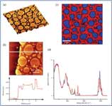
The topographic image obtained with the AFM (Figure 2a) reveals round features 20-30 nm in height with a diameter varying from 150 nm to 4 µm surrounded by a network-like structure. To determine the height of the PMMA-SBR film, the polymer was scratched off from a part of the film with a fine needle and imaged again as shown in Figure 2b. The cross section (marked with a white line) in the AFM image shows that the low areas of the blend have a height of about 30 nm, while the round features are up to 70 nm in height.

Figure 2. (a) AFM image of a PMMA-SBR polymer blend, spin coated on glass. 20 à 20 µm scan, 30 nm topography scale. (b) To determine the height of the PMMA-SBR film, the polymer was scratched off from a part of the film. The cross section (marked with a white line) in the AFM image shows that the low areas of the blend have a height of about 30 nm, while the round features are up to 70 nm in height. (c) Raman image of the PMMA-SBR polymer blend. The PMMA is color coded blue, whereas the SBR is shown in red. Imaging parameters: 200 à 200 spectra, 70 ms integration time per spectrum. (d) Raman spectra obtained from areas with (red) SBR and (blue) PMMA, respectively. The broad double peak up to 1500 cm-1 is due to the glass substrate. Without confocal detection, this peak would completely hide the polymer spectra.
From the AFM measurements, the phase separation can be seen clearly but it cannot be determined whether the phases are separated completely and which material forms the round features and which the network. A Raman image of the structure (Figure 2c) reveals the chemical structure of the phases. The Raman image was obtained using a 100×, NA = 1.25 oil immersion objective with 532 nm excitation. The image consists of 200 × 200 spectra taken with 70 ms integration time per spectrum. One can see clearly the complete phase separation of the polymers. It is obvious also that the PMMA forms the round, flat structures while the rubber is present in the network structures.
Figure 2d shows Raman spectra obtained in the PMMA and the SBR areas, respectively. The broad double peak at up to 1500 cm-1 is due to the glass substrate. If the measurement were taken without confocal detection, the glass background would have been more than a factor of 100 higher, completely covering the Raman lines of the polymers. Note that even an only 30-70 nm thin polymer film provides enough intensity to analyze structural differences less than 100ms integration time per spectrum.
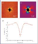
Stress measurements. Figure 3a shows an AFM measurement of a Vickers indent into silicon. A Vickers tip is used for hardness testing. By measuring the diagonal size of the indent applied with a known force, the hardness of the sample can be determined. Usually, the size of the indent is measured with an optical microscope. However, if the hardness of a thin coating has to be measured, the indent should not be deeper than approximately one tenth of the thickness of the coating. Otherwise, the substrate influences the result. For thin coatings, the indent must be extremely shallow and therefore small so that size measurements with an optical microscope can be very inaccurate.

Figure 3. (a) AFM measurement of a Vickers indent into silicon. The indent with 2.75 µm diagonal and 210 nm depth was performed with a force of 50 mN. Scan area: 10 µm à 10 µm. The topography scale in the image is only 10 nm. (b) Raman image of the same scan area as in (a). The image was calculated by determining the peak position of a parabolic fit of the Si-Raman line of each measured spectrum. Imaging parameters: 100 à 100 spectra, 70 ms integration time per spectrum. Excitation: 10 mW at 532 nm, objective: 100Ã, NA = 0.9. (c) Stress along the line indicated in (b). The RMS noise of 0.021 cm-1 corresponds to a stress resolution of 9 MPa in Si.
In this case, the Vickers indent was performed with a force of 50 mN and produced an indent with 210 nm depth and 2.75 µm diagonal size as extracted from the AFM measurement. A close inspection also reveals a small anisotropy of the indent, which is due to the limited precision of the shape of the Vickers diamond.
The indent produces a stress field that was imaged with Raman spectroscopy. If, for example, a compressive stress is applied to a sample, the binding distance of the atoms is reduced resulting in a higher vibrational frequency. The Raman line of this vibration therefore is shifted to higher frequencies. Accordingly, a tensile strain shifts the Raman lines to lower wavenumbers.
The image shown in Figure 3b was calculated by determining the peak position of a parabolic fit of the Si-Raman line of each measured spectrum. The scan area is 10 µm × 10 µm and 100 × 100 = 10,000 spectra were taken with an integration time of 70 ms per spectrum. For excitation and detection, a 100×, NA = 0.9 objective (diffraction-limited spot size 360 nm, pixel size 100 nm) and about 10 mW of power from a frequency-doubled Nd:YAG laser at 532 nm was used. The spectra were obtained with a 300 mm imaging spectrometer equipped with an 1800 lines/mm grating and a back-illuminated CCD camera. The complete image acquisition took less than 17 min.
As expected, the stress field as shown in Figure 3b has the symmetry of the Vickers pyramid. The tensile strain appears along the edges of the pyramid, while the compressive strain appears at the flat sides.
Assuming uniaxial strain, the relation between Raman peak shift and stress in Si is σ(MPa) = -435 Δω (1/cm). The standard deviation of the peak shift of the Si-Raman line as derived from the image is 0.021 cm-1, corresponding to a stress sensitivity of only 9 MPa for the experimental conditions mentioned earlier. With longer integration times, even higher accuracy can be achieved. The strain is calculated using the above formula for the cross section in Figure 3c.
Summary
As shown in the examples here, confocal Raman microscopy is a powerful tool for the analysis of heterogenous samples on the submicrometer scale. If the CRM is combined with an atomic force microscope, the lateral resolution is extended to the nanometer scale and the ultimate resolution of the AFM can be combined with the chemical information obtained by the CRM. The combination of both methods is an ideal tool for the growing field of nanotechnology.
Olaf Hollricher is managing director, Wolfram Ibach is a research and development specialist, Ute Schmidt is an applications manager, and Joerg Mueller is a production manager, for WITec GmbH (Ulm, Germany). E-mail: Olaf.Hollricher@WITec.de.

High-Speed Laser MS for Precise, Prep-Free Environmental Particle Tracking
April 21st 2025Scientists at Oak Ridge National Laboratory have demonstrated that a fast, laser-based mass spectrometry method—LA-ICP-TOF-MS—can accurately detect and identify airborne environmental particles, including toxic metal particles like ruthenium, without the need for complex sample preparation. The work offers a breakthrough in rapid, high-resolution analysis of environmental pollutants.
New Study Reveals Insights into Phenol’s Behavior in Ice
April 16th 2025A new study published in Spectrochimica Acta Part A by Dominik Heger and colleagues at Masaryk University reveals that phenol's photophysical properties change significantly when frozen, potentially enabling its breakdown by sunlight in icy environments.
AI-Driven Raman Spectroscopy Paves the Way for Precision Cancer Immunotherapy
April 15th 2025Researchers are using AI-enabled Raman spectroscopy to enhance the development, administration, and response prediction of cancer immunotherapies. This innovative, label-free method provides detailed insights into tumor-immune microenvironments, aiming to optimize personalized immunotherapy and other treatment strategies and improve patient outcomes.